Having successfully removed the RAM chips from the 16500A’s processor board without wrecking either the chips or the board, it’s time to try and wire up the replacement memory. I have a 4MB SIMM to replace it with. A little web searching reveals the SIMM pinout:
| PIN | SYMBOL | PIN | SYMBOL | PIN | SYMBOL | PIN | SYMBOL |
|---|---|---|---|---|---|---|---|
| 1 | Vss | 19 | A10 | 37 | NC | 55 | DQ12 |
| 2 | DQ1 | 20 | DQ5 | 38 | NC | 56 | DQ28 |
| 3 | DQ17 | 21 | DQ21 | 39 | Vss | 57 | DQ13 |
| 4 | DQ2 | 22 | DQ6 | 40 | CAS0# | 58 | DQ29 |
| 5 | DQ18 | 23 | DQ22 | 41 | CAS2# | 59 | Vdd |
| 6 | DQ3 | 24 | DQ7 | 42 | CAS3# | 60 | DQ30 |
| 7 | DQ19 | 25 | DQ23 | 43 | CAS1# | 61 | DQ14 |
| 8 | DQ4 | 26 | DQ8 | 44 | RAS0# | 62 | DQ31 |
| 9 | DQ20 | 27 | DQ24 | 45 | NC/RAS1#* | 63 | DQ15 |
| 10 | VDD | 28 | A7 | 46 | NC | 64 | DQ32 |
| 11 | NC | 29 | NC (A11) | 47 | WE# | 65 | DQ16 |
| 12 | A0 | 30 | VDD | 48 | NC | 66 | NC |
| 13 | A1 | 31 | A8 | 49 | DQ9 | 67 | PRD1 |
| 14 | A2 | 32 | A9 | 50 | DQ25 | 68 | PRD2 |
| 15 | A3 | 33 | NC/RAS3#* | 51 | DQ10 | 69 | PRD3 |
| 16 | A4 | 34 | RAS2# | 52 | DQ26 | 70 | PRD4 |
| 17 | A5 | 35 | NC | 53 | DQ11 | 71 | NC |
| 18 | A6 | 36 | NC | 54 | DQ27 | 72 | Vss |
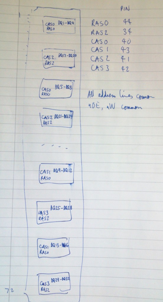
That’s all very useful, but I need to know how the chips are wired up and how the various RAS and CAS lines on the SIMM correspond with the chips themselves. Time for the continuity tester again. A few minutes of beeping reveals the arrangement:
To summarise:
- The SIMM is 32 bits wide, and each of the 8 chips handles 4 bits. The 16500A wants 16 bit wide RAM, so half the data pins will have to be commoned together. The layout of the SIMM connector actually makes this quite easy, because the data bits are interleaved in what looks like a handy fashion.
- the nW line is common to all the chips. The 16500A wants two separate nW lines, so I’ll have to cut the track half way along the SIMM. There seems to be a convenient point under where the parity RAM would be if the SIMM had parity, which it doesn’t.
- There are two RAS lines used. The 16500A only wants one, so they’ll be commoned together.
- There are four CAS lines, one for every two chips. The 16500A wants two, so they will be wired as two pairs.
Here’s the plan of action To understand the references to signals in the 16500A, see the previous post.
- Split nWE half way along the SIMM and connect top half to 16500A W0, bottom half to 16500A W1
- Connect 16500A CAS0 to SIMM CAS3 and CAS2
- Connect 16500A CAS1 to SIMM CAS1 and CAS0
- Connect 16500A D7..D4 to SIMM DQ1..DQ4 and DQ17..DQ20
- Connect 16500A D3..D0 to SIMM DQ5..DQ8 and DQ21..DQ24
- Connect 16500A D15..D12 to SIMM DQ9..DQ12 and DQ25..DQ28
- Connect 16500A D11..D8 to SIMM DQ13..DQ16 and DQ29..DQ32
- Connect 16500A A9..A0 to SIMM A9..A0
- Connect 16500A nOE to SIMM nOE
- Connect 16500A RAS to SIMM RAS0 and RAS2
- Connect power and ground
- Cross fingers.
