Category Archives: HP 16500A/B

HP 16534A triggering problems

DSC_0404

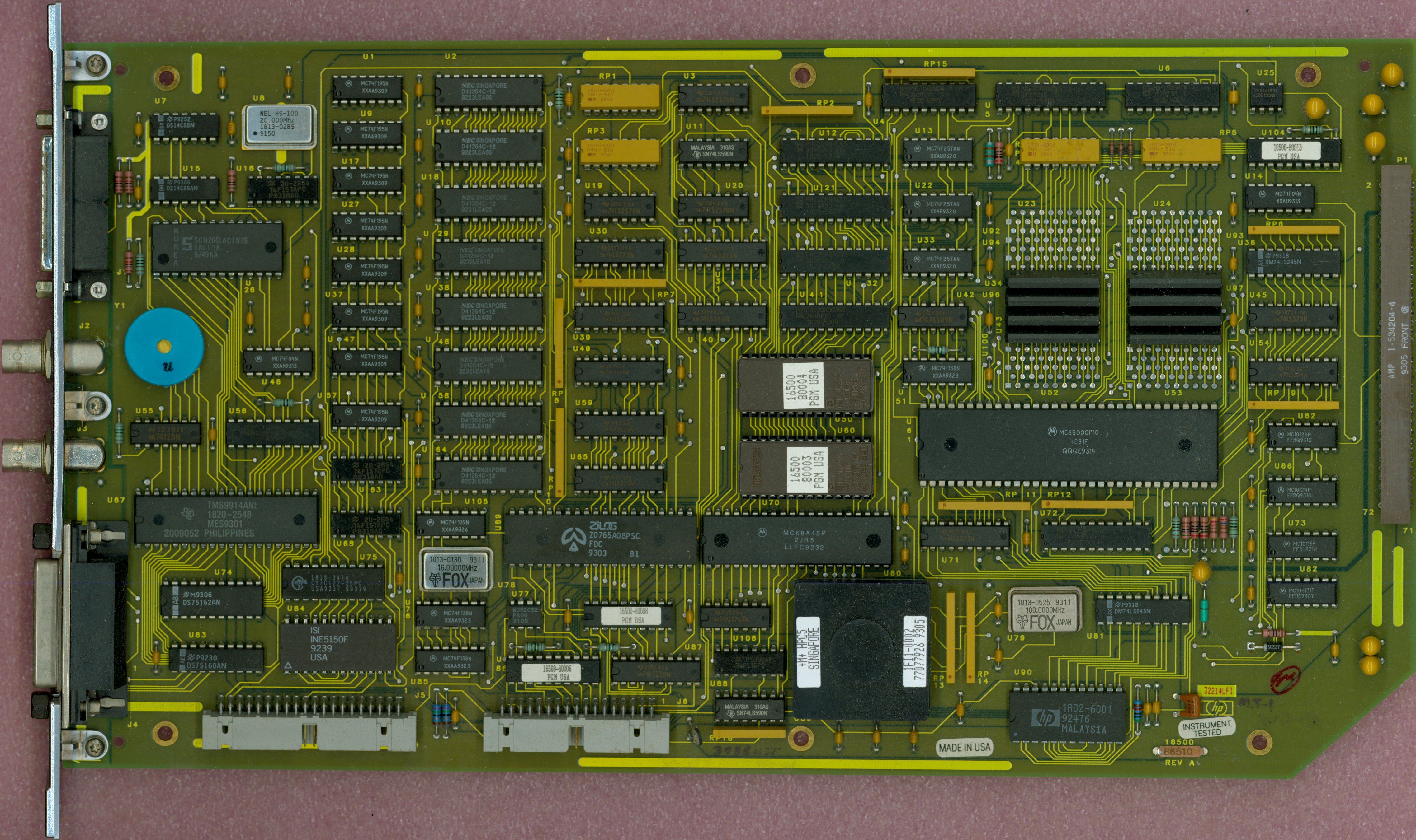
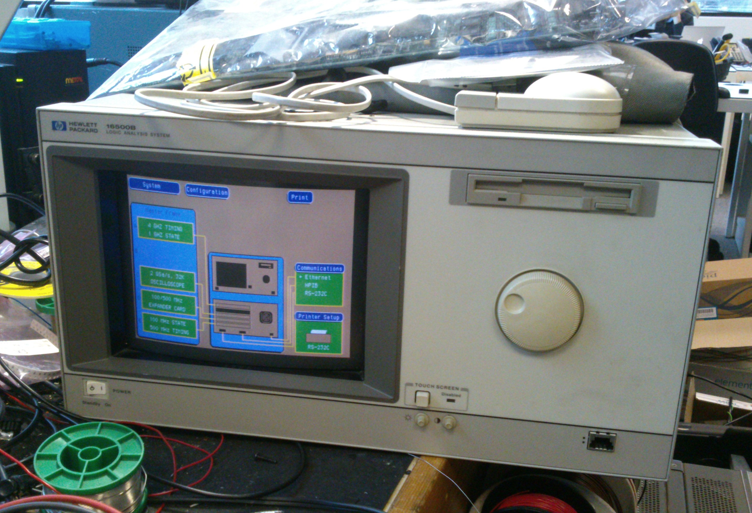
One of my HP 16500B logic analysis systems has a 16534A digital oscilloscope module installed. The module has a great specification: two channels, 2Gsamples/sec, 500MHz analogue bandwidth, and 32k record length. I would find it a really useful debugging tool, if it worked properly. Sadly it doesn’t.

Though it displays a trace successfully, and the controls work, it won’t trigger. The only way I get a trace is by auto-trigger. In this case the trace isn’t synchronised, so it’s impossible to catch a particular event at a particular time. Here it is displaying a square wave (well, it’s nearly square – I hadn’t adjusted the probe compensation so it’s a bit curvy on the top and bottom). Adjusting the trigger level just doesn’t make any difference.

DSC_0409

The service manual for the 16534A isn’t very helpful. It describes roughly what the self-tests do, and how to run the self-calibration procedure, but has no detailed circuit information. The self-test reports a ‘D/A’ failure:

DSC_0405and the self-calibration procedure fails on the Trigger and Hysteresis sections:

DSC_0406

The service guide describes the D/A test like this:

Test DAC This test verifies the correct operation of the D/A convertor on the board.
Both the offset and trigger level D/A convertors for each channel are set to a reference
level and then changed. The logic trigger IC is programmed to detect the changes. The
detection of a correct trigger indicates that the D/A convertor is operating normally.

It seems clear that the offset D/A converter is working, since the offset control works and moves the trace up and down as it should. However, the trigger level control doesn’t seem to be doing what it should. I had a look at the board, looking for components likely to be the DAC or trigger IC. Unfortunately, the semiconductors on there seem to be mostly either standard ECL logic, trivial things like op-amps, or magic custom HP chips with dozens of pins. One exception was this:

DSC_0410

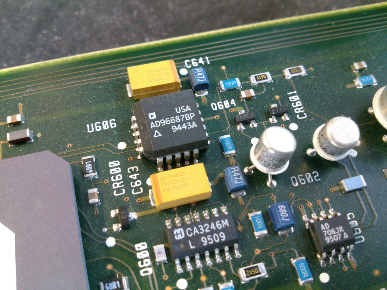
It’s an AD96687 from Analog Devices, which is a dual high-speed comparator with ECL outputs. If I was designing a high-speed trigger circuit using 1994-vintage components, I might use a device like this. I’ve had a look at all its pins with the power switched on and a signal applied and tests running, and none of them seem to change at all. One noninverting input is stuck at +5V, and the other inputs are near ground. One set of outputs isn’t even showing valid ECL logic levels, but it may be unused and thus have no load resistors on it.

Maybe it’s a red herring and nothing to do with the triggering at all, but I’m suspicious that I never see anything change. Without more circuit information, it’s hard to get much further, sadly.


HP 16500A memory upgrade part 7

In part 6, I established that something was stopping the floppy disc drives in my 16500A working when I changed the ROMs to software version 00.02. Thanks to the help of some on the hp-agilent-equipment Yahoo group, especially Glen Slick, I have determined that there’s an important difference between early CPU boards running 00.00 and later ones running 00.02: the floppy disc controller chip has changed!

The old board has an FDC9793 and the new one a uPD765 (or at least its Zilog equivalent). There are pictures of all the boards here. Now, I started to wonder, could I somehow fit the uPD765 to my board? It seems crazy and would only make sense if it wasn’t possible to exchange the whole board. So I started investigate. As luck would have it I have a functional 16500B with a logic analyzer plugin, so I could have a look and see what was going on around the disc controller on my CPU board. I wired up the relevant pins of the FDC9793.

DSC_0305

Examining the logic analyzer trace, it seems that the CPU is trying to read something from the disc controller, which is at least a start.

DSC_0304

It’s reading from what would be the status register repeatedly, as if waiting for some condition to be true. It gets a value of 0x04 every time, which is presumably not what it wants. It does this at the right stage of the self-test. I thought this was promising, since it is at least addressing the chip. Might it be possible to wire one in place of the other? Their pinouts are different. Comparing them, using their datasheets:

FDC9793 uPD765
1 RESET I active high
2 nWE I nRD I
3 nCS I nWR I
4 nRE I nCS I
5 A0 I D/nS I data/nStatus register select
6 A1 I D0 I/O
7 D0 I/O D1 I/O
8 D1 I/O D2 I/O
9 D2 I/O D3 I/O
10 D3 I/O D4 I/O
11 D4 I/O D5 I/O
12 D5 I/O D6 I/O
13 D6 I/O D7 I/O
14 D7 I/O DRQ O DMA request
15 STEP O Step output nDACK I DMA ack
16 DIRC O Direction (high=in, low=out) TC I end of DMA transfer
17 EARLY O write precompensation IDX I index pulse
18 LATE O write precompensation INT O interrupt output
19 nMR I master reset CLK I 8MHz
20 GND GND
21 +5V WCK I write clock
22 nTEST I tie to +5V RDW I read data window
23 HLT I input, head engaged RDD I read data from data sep
24 CLK I 1MHz in VCO/SYNC O enable VCO
25 RG O read gate to data sep WE O write enable
26 RCLK I read clock from data sep MFM O MFM/FM
27 nRAW READ I raw data from drive HD O head select
28 HLD O head load US1 O unit select
29 TG43 O track greater than 43 US0 O unit select
30 WG O write gate WDA O write data
31 WD O write data PS1 O precompensation shift (early/late/normal)
32 READY I ready PS0 O precompensation shift (early/late/normal)
33 nWF I/O write fault/vfo en to data sep FLT/TR0 I track 0/fault
34 nTR00 I track 0 WP/TS I write protect/two side
35 nIP I index pulse RDY I drive ready
36 nWPRT I write protect HDL O head load
37 nDDEN I double density FR/STP O fault reset/step
38 DRQ data req, open-collector LCT/DIR O low current/direction
39 INTRQ interrupt req, open-collector nRW/SEEK O indicates seek/read/write mode
40 +5V

There are some important differences here. Firstly, the uPD765 expects an 8MHz clock where the FDC9793 used a 1MHz clock. That’s not a good start. The uPD765 includes drive and side select logic, but the FDC9793 doesn’t. The two also differ a lot in how they handle things like write precompensation signals, and the uPD765 effectively multiplexes various signals too.

At this point I think the swap is just too difficult. It becomes cheaper and easier to swap the whole CPU board, if I can find one, or simply upgrade the whole machine to be a 16500B.

HP 16500A CPU board versions

As part of my quest to upgrade my HP 16500A logic analyser’s memory, I’ve found out more than I ever expected about the various versions of the 16500A CPU board. I’ve been fortunate to have the help of the good people of the [hp_agilent_equipment] Yahoo! group. My most recent stumbling block has been that installing ROM version 00.02 in my (early) 16500A stops the floppy disc drives working.

Glen Slick, from the above group, was kind enough to send me high-resolution scans of the two 16500A CPU boards he has. That makes three known versions, and here I’ll post pictures of them and attempt a description of the differences.

16500-66503 with 1MB RAM

DSC_0262

This is the board from my machine. It has 1MB RAM in 8 TMS44C256-12N DIL chips, and the floppy disc controller is a Standard Microsystems FDC9793. The ROMs contain software version 00.00. For completists, I have put images of the V00.00 16500A ROMs here.

16500-66507 with 2.5MB RAM

16500-66507-FRONT

This is one of Glen’s boards. It has 2.5MB RAM fitted as 20 off TC514256AZ-10 1Mbit ZIP chips, and the floppy disc controller is a Zilog Z0765A (which seems to be compatible with the very common uPD765 as found in the original IBM PC). The ROMs contain software version 00.02. It also has three extra programmable devices with labels on them. The details of their encapsulation mouldings look very similar to PALs elsewhere on the board, but why don’t all the PALs have labels on them? The labelled ones are:

  • 16500-80006, U86, by the floppy drive connector at the bottom
  • 16500-80007, U104, top right
  • 16500-80008, no designator visible, next to the floppy controller IC

16500-66510 with 4MB RAM

16500-66510-FRONT

This is another of Glen’s boards. The part number (66510) seems to be on a sticker. The only noticeable difference, other than the RAM chip complement, from the 66507 board is that the chip top right is labelled 16500-80013. It has 4MB of RAM as 8 off TC514400AZ-80 4Mbit ZIP chips. The ROMs contain software version 00.02.

HP 16500A memory upgrade part 6

In part 5, upgrading the software on my 16500A’s CPU board to version 00.02 resulted in a self-test failure, which wasn’t fixed by downgrading back to 00.00. I’ve just had a look to see why that was happening.

The front panel is connected to the backplane by a 10-way connector. I traced out the pinout of the connector:

  1. +5V power
  2. +12V power
  3. +5V power
  4. +12V power
  5. Ground
  6. Data
  7. Ground
  8. Data
  9. Ground
  10. On/off switch, ground to switch system off

There was no activity at all on pins 6 and 8, the data pins, even during self-test. I traced them through to the CPU board via pins 59 and 60 of the CPU board’s backplane connector, and thence to U90 pins 18 and 19. This is an HP custom chip. There seemed to be activity on many of its pins, but nothing on those two. Poking around, I found that two of its pins are connected to a nearby ceramic resonator which clearly wasn’t resonating. Aha! Got it. One of the pins of the resonator had broken. I soldered it back together and now the self-tests pass!

But there’s a fly in the ointment. V00.02 software doesn’t seem to be able to access the floppy disc drives, simply reporting ‘No Disc’ for both of them even when they’ve got discs in.

Looking at the floppy disc connector with a scope, the ‘drive select’ pins are definitely active. It seems that the pinout of Sony 3.5″ floppy disc drives changed at some point. The details are here:

http://www.retrotechnology.com/herbs_stuff/drive.html#35new

Pin#  Signal (Old Sony)  Signal (New Sony)  Pin#  Signal (Old Sony)        Signal (New Sony)
1     Disc Change Reset   NC                2     Disc Change Indicator    NC
3     +5V                 Key               4     Density Bit              NC
5     +5V                 Ground            6     Drive Select             NC
7     +5V                 Ground            8     Index Pulse              Index
9     +5V                 Ground            10    Drive Select 0           NC
11    +5V                 Ground            12    Drive Select 1           Drive Select 1
13    Ground              Ground            14    Drive Select 2           NC
15    Ground              Ground            16    Motor On                 Motor On
17    Ground              Ground            18    Direction Select         Direction
19    Ground              Ground            20    Step                     Step
21    Ground              Ground            22    Write Data               Write Data
23    Ground              Ground            24    Write Gate               Write Gate
25    Ground              Ground            26    Track 0 Indicator        Track 00
27    Ground              Ground            28    Write Protect Indicator  Write Protect
29    +12V                Ground            30    Read Data                Read Data
31    +12V                Ground            32    Head Select              Head 1 Select
33    +12V                Ground            34    Ready                    Disc Change

It seems that the ‘disc change indicator’ has moved at some point in the history of Sony disc drives. Maybe the new software is expecting to see the ‘disc change’ indicator before it tries to switch the drive motors on? Grounding pin 34 doesn’t seem to make any difference. The disc controller is an FDC9793. Looking up the data sheet on it, it doesn’t have any means of indicating whether a disc is in or not. Without a schematic, it’s going to be very hard to figure out how the software determines it.

HP 16500A memory upgrade part 5


Following on from part 4, I’ve now tried a newer software version in the 16500A’s EPROMs. Finding a couple of good 27C256s with 200ns access time took a few minutes, but there were no problems with the programming. So, I put them in the CPU board, reinstalled it in the mainframe, and switched on:imageOh dear. That’s not good. Without HIL (which is the socket for mouse and keyboard on the front), front panel (which I assume is the spinner knob) or touchscreen, the machine isn’t a lot of use. Must be a compatibility problem with the new software version, I think to myself. Swap in the old ROMs – and the problem is still there. Check the wiring to the front panel, all looks good.

This is annoying. I wasn’t expecting new faults with the hardware. When I next get time to spend on it, I’ll do the obvious checks for bent pins and so on.


HP 16500A memory upgrade part 4

Having worked out the wiring for a 4MB SIMM to the 16500A CPU board in part 3, I got out the mod wire and soldered it all together.

DSC_0281

It all went together quite easily. The pins, even on the SIMM, are so much further apart than modern surface-mount components that I’m used to dealing with. Notice the red wire running along the row of chips on the SIMM: that’s nOE, where I had to lift pin 16 of each chip and wire them together because the original SIMM tracks grounded them. I also cut the track joining all the pin 3’s (nWE) of the chips together, half way along the SIMM, so that the upper four chips had a separate nWE from the lower four, again because that’s the way the CPU board expected them.

Having checked and double-checked the wiring, I plugged the board into the mainframe and switched on. Much to my amazement, I heard the sound of the floppy drives seeking almost immediately. It was running! Once the monitor had warmed up, I could see that the mainframe was booting absolutely normally. It passed all its self-tests. But, did it recognise the extra memory? With some trepidation I stabbed the screen to select test mode and looked at the bottom line of the display:

DSC_0284


Oh dear. Just 1MB then. Serves me right for trying to make a silk purse out of a sow’s ear. I suspect ROM version 00.00 (what kind of a version number is that?) doesn’t support more than this, since later 16500As had a different ROM version and more memory. Just for kicks, I popped in the test disk and tried the proper memory test:

DSC_0283


At least the new RAM works as well as the old stuff did, even if it isn’t any bigger. I haven’t broken it, but I haven’t improved it either. I also tried loading the 16550A module software, just in case it was somehow able to find the extra RAM even if the rest of the system didn’t know about it, but it still reported that there wasn’t enough space.

I think my next quest will be to find a copy of the later ROM and program a couple of EPROMs with it. A quick Google search for ‘16500A ROM’ reveals this site:

http://www.jammarcade.net/hp-16500a-logic-analyser/

with an image of the later ROMs. When I get a moment, I’ll program up a pair of 27C256As and see what happens…


HP 16500A memory upgrade part 3

I’ve worked out the wiring of the SIMM to the CPU board. Unfortunately, the OE signal on the SIMM is hard-wired to ground, which is annoying. I’ll have to lift the legs (pin 16) of each of the RAM chips and hand-wire them together.

This is completely untested…

Signal 16500A chip pin SIMM signal SIMM pins
. GND all 20 VSS 1, 39, 72
. Vss all 10 VDD 10, 30, 59
. D0 U43, U52 19 DQ8, DQ24 26, 27
. D1 U43, U52 18 DQ7, DQ23 24, 25
. D2 U43, U52 2 DQ6, DQ22 22, 23
. D3 U43, U52 1 DQ5, DQ21 20, 21
. D4 U23, U34 2 DQ4, DQ20 8, 9
. D5 U23, U34 1 DQ3, DQ19 6, 7
. D6 U23, U34 19 DQ2, DQ18 4, 5
. D7 U23, U34 18 DQ1, DQ17 2, 3
. D8 U44, U53 2 DQ16, DQ32 65, 64
. D9 U44, U53 1 DQ15, DQ31 63, 62
. D10 U44, U53 18 DQ14, DQ30 61, 60
. D11 U44, U53 19 DQ13, DQ29 57, 58
. D12 U24, U35 19 DQ12, DQ28 55, 56
. D13 U24, U35 18 DQ11, DQ27 53, 54
. D14 U24, U35 1 DQ10, DQ26 51, 52
. D15 U24, U35 2 DQ9, DQ25 49, 50
. W0 U23, U34, U43, U52 3 nWE 47 (top half)
. W1 U24, U35, U44, U53 3 nWE 47 (bottom half)
. RAS all 4 RAS0, RAS2 44, 34
. CAS0 U23, U24, U52, U53 17 CAS3, CAS2 42, 41
. CAS1 U34, U35, U43, U44 17 CAS1, CAS0 43, 40
. OE all 16 wire separately
. A0 all 6 A0 12
. A1 all 7 A1 13
. A2 all 8 A2 14
. A3 all 9 A3 15
. A4 all 11 A4 16
. A5 all 12 A5 17
. A6 all 13 A6 18
. A7 all 14 A7 28
. A8 all 15 A8 31
. A9 all 5 A9 32

HP 16500A memory upgrade part 2

Having successfully removed the RAM chips from the 16500A’s processor board without wrecking either the chips or the board, it’s time to try and wire up the replacement memory. I have a 4MB SIMM to replace it with. A little web searching reveals the SIMM pinout:

PIN SYMBOL PIN SYMBOL PIN SYMBOL PIN SYMBOL
1 Vss 19 A10 37 NC 55 DQ12
2 DQ1 20 DQ5 38 NC 56 DQ28
3 DQ17 21 DQ21 39 Vss 57 DQ13
4 DQ2 22 DQ6 40 CAS0# 58 DQ29
5 DQ18 23 DQ22 41 CAS2# 59 Vdd
6 DQ3 24 DQ7 42 CAS3# 60 DQ30
7 DQ19 25 DQ23 43 CAS1# 61 DQ14
8 DQ4 26 DQ8 44 RAS0# 62 DQ31
9 DQ20 27 DQ24 45 NC/RAS1#* 63 DQ15
10 VDD 28 A7 46 NC 64 DQ32
11 NC 29 NC (A11) 47 WE# 65 DQ16
12 A0 30 VDD 48 NC 66 NC
13 A1 31 A8 49 DQ9 67 PRD1
14 A2 32 A9 50 DQ25 68 PRD2
15 A3 33 NC/RAS3#* 51 DQ10 69 PRD3
16 A4 34 RAS2# 52 DQ26 70 PRD4
17 A5 35 NC 53 DQ11 71 NC
18 A6 36 NC 54 DQ27 72 Vss

That’s all very useful, but I need to know how the chips are wired up and how the various RAS and CAS lines on the SIMM correspond with the chips themselves. Time for the continuity tester again. A few minutes of beeping reveals the arrangement:

DSC_0276

To summarise:

  • The SIMM is 32 bits wide, and each of the 8 chips handles 4 bits. The 16500A wants 16 bit wide RAM, so half the data pins will have to be commoned together. The layout of the SIMM connector actually makes this quite easy, because the data bits are interleaved in what looks like a handy fashion.
  • the nW line is common to all the chips. The 16500A wants two separate nW lines, so I’ll have to cut the track half way along the SIMM. There seems to be a convenient point under where the parity RAM would be if the SIMM had parity, which it doesn’t.
  • There are two RAS lines used. The 16500A only wants one, so they’ll be commoned together.
  • There are four CAS lines, one for every two chips. The 16500A wants two, so they will be wired as two pairs.

Here’s the plan of action To understand the references to signals in the 16500A, see the previous post.

  • Split nWE half way along the SIMM and connect top half to 16500A W0, bottom half to 16500A W1
  • Connect 16500A CAS0 to SIMM CAS3 and CAS2
  • Connect 16500A CAS1 to SIMM CAS1 and CAS0
  • Connect 16500A D7..D4 to SIMM DQ1..DQ4 and DQ17..DQ20
  • Connect 16500A D3..D0 to SIMM DQ5..DQ8 and DQ21..DQ24
  • Connect 16500A D15..D12 to SIMM DQ9..DQ12 and DQ25..DQ28
  • Connect 16500A D11..D8 to SIMM DQ13..DQ16 and DQ29..DQ32
  • Connect 16500A A9..A0 to SIMM A9..A0
  • Connect 16500A nOE to SIMM nOE
  • Connect 16500A RAS to SIMM RAS0 and RAS2
  • Connect power and ground
  • Cross fingers.

HP 16500A memory upgrade part 1

My HP 16500A has only 1MB of RAM, which isn’t enough to run the system software for the 16550A logic analyzer module I’d like to use in it. Apparently there was a later version of the 16500A which had 2.5MB of RAM, but I haven’t got one of those. Just my luck. Trying to load the 16550A system software results in an error message:

DSC_0273a

This got me thinking. Might I be able to upgrade the memory? The RAM on the 16500A processor board is eight 1Mbit DRAM chips, soldered in:

16500A_RAM

I looked up the data sheet for the chips, TMS44C256. It indicates that pin 5 isn’t used. However, on larger (4Mbit) chips, pin 5 is another address line. Intriguingly, pin 5 is wired up on this processor board, implying that the hardware is ready for larger RAM chips. I have no idea whether the software is ready, but there’s only one way to find out. It’s got to be worth a try, hasn’t it?

Unfortunately I couldn’t find any 4Mbit DRAM chips in the DIL package to fit this board, and making or buying adapters for surface mount chips seems like a pain. However, there is another approach: old PCs are full of SIMM memory modules which have electrically suitable chips on them, and they’re already wired conveniently together. If I removed the 1Mbit DRAM chips from the processor board and string wires from the resulting holes to a SIMM, I might have a 4MB 16500A. Or a doorstop.

To change DRAM chips requires knowing how the address and data buses are wired, and how the RAS and CAS strobe lines are connected to the various chips. RAS and CAS are effectively chip enables, so they can be considered to be part of the address for wiring purposes. A bit of reverse engineering with a continuity tester resulted in this sketch of how the RAM is wired up:

DSC_0253

If I do a similar job on a suitable 72-pin 4MB SIMM, it should be possible to match up the wires and see what happens. There’s a handy vintage SIMM data sheet I found here:

http://www.pjrc.com/mp3/simm/datasheet.html

which should be a good start. What can possibly go wrong?

HP 16500A and 16500B logic analysers

Recently I’ve been putting a couple of HP logic analysis systems into action. Accumulated from various places over the last couple of years I have both a 16500A and a 16500B. They’re remarkable units which take a whole variety of plugins for doing high-speed digital and analogue measurements. They must have been eye-wateringly expensive when new and, as a result, have such high specifications that they’re still useful even though they’re around 20 years old. For example, the 16500B boasts a colour touch-screen, a built-in hard drive and Ethernet. It was launched in 1992 when many desktop PCs didn’t have those features, so it must have seemed awesomely high-tech at the time.

Here’s a picture of the 16500B. The 16500A is similar but looks…older.

DSC_0247s

There are a few quirks to using these machines in 2013, and I’m intending to write about some of my experiences here.