Monthly Archives: February 2013

Motorboating in Space

zaxxon3

Or, how to stop Zaxxon going thump-thump-thump.

‘Motorboating’ has been a problem in electronics almost as long as electronics has existed. It gets its name from a characteristic thumping or buzzing noise, reminiscent of a motor boat’s engine. It’s a problem which usually occurs in audio amplifiers, and it happens either because of a design error or faulty components. Sometimes a change in an amplifier’s operating environment, such as a radio battery running down, can cause it. It’s loud, annoying, and can even damage speakers,

The reason for the noise is feedback. If an amplifier drives a signal into a loudspeaker, the power for that signal has to come from its power supply. Its power supply, especially if it’s a run-down radio battery, isn’t perfect. Drawing power from it makes its output drop in voltage for a moment. Unfortunately, electronic circuits aren’t perfect either. Their behaviour is strongly affected by their power supply. Connect such a circuit to such a power supply and amplifier, and you have a vicious circle: circuit sends a signal to amplifier, amplifier sends it to speaker and draws more power, power supply affects circuit, which makes another signal which gets sent to amplifier, and so on. It’s called feedback because the output signal feeds back into the input, via an unorthodox route. The circle of feedback can lead to the regular buzzing noise – the motorboating.

Recently I have restored a Zaxxon arcade game circuit board, which dates from 1982 (actually, it’s a bootleg, but the circuit is largely the same). I got it working well, but with one big problem: the sound was accompanied by a constant thumping noise which wasn’t supposed to be there. Here’s a short movie of how it sounded. It’s especially noticeable at the start and end of the clip.

Fans of the game will know that Zaxxon has very distinctive sound. Many video games at the time used digital techniques, often using standard chips, to generate their sound, which gives them a characteristic bleepy quality. Zaxxon is different. It uses what amounts to an analogue synthesizer: a magnificent assembly of timers, oscillators, amplifiers and filters. It has a lot in common with the kind of instruments used in pop music at the time. It makes a glorious, raucous noise.

IMG_3560

But this kind of analogue circuitry has a problem, especially when it’s cheaply built using early 1980s technology: it’s very sensitive to its power supply. Any variation in the power supply basically gets straight to the synthesizer’s output. What’s more, Zaxxon’s loudspeaker amplifier runs from the same power supply as the synthesizer. This lot is a recipe for motorboating, and that’s exactly what happened to my game.

zaxxon-power-1

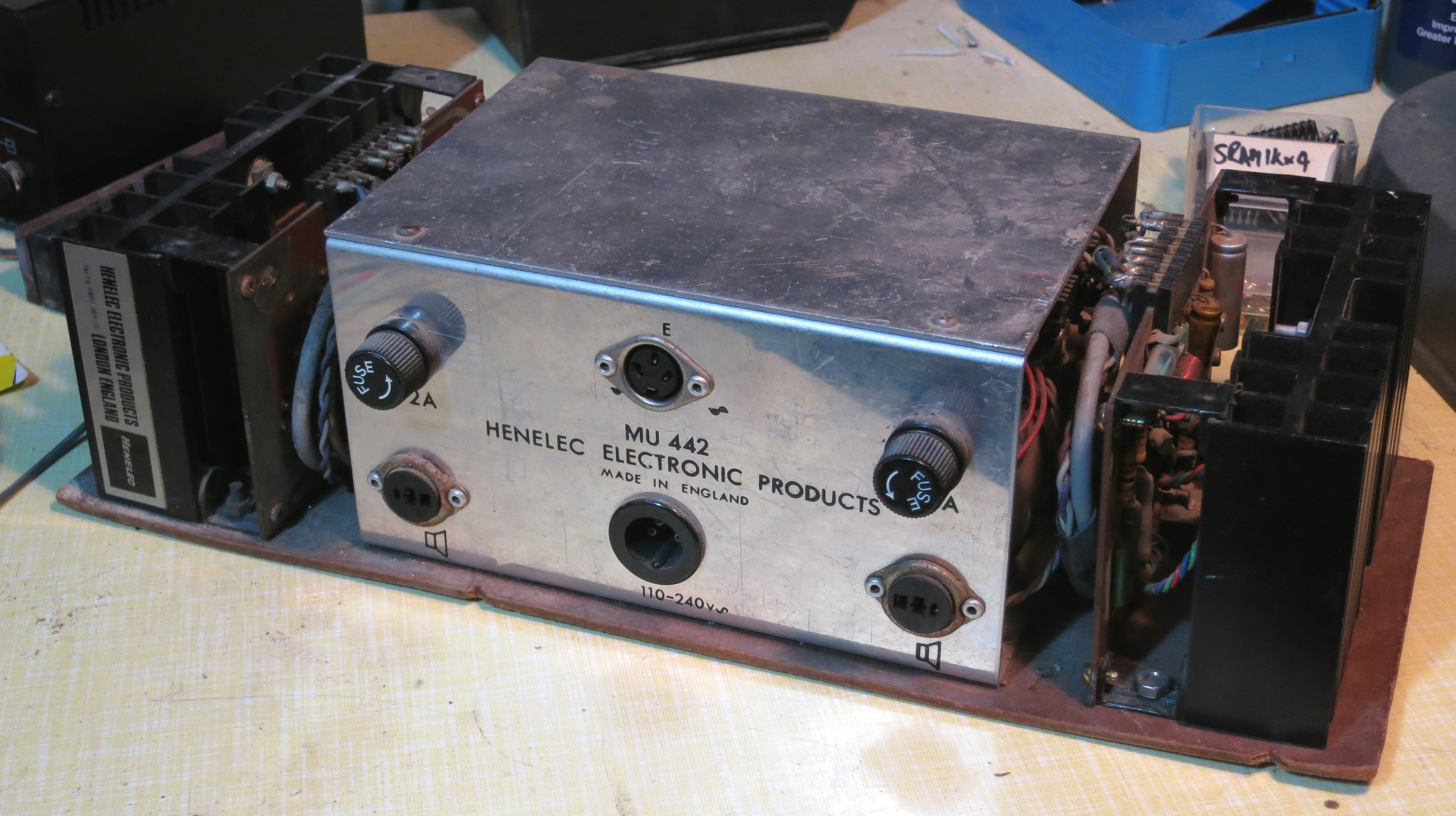
Of course, we have to assume that it all worked properly when it came out of the factory, but then it would have been running from an official Zaxxon power supply. The one I use in my arcade game test rig may not be as good as the original one, but it’s good enough for most things, and I wasn’t going to change it just to fix this problem. So I had to come up with a modification to keep apart the amplifier power and the synthesizer power.

The traditional cheap and cheerful way of keeping power supplies apart, known as decoupling them, is simply to put a resistor and capacitor between them, like this:

DSC_0335

This decoupling means that variations in one power supply have a smaller effect on the other. It works well, and has been used in millions of electronic devices from the earliest days of radio. However, a certain amount of power is always lost in the resistor. Many circuits don’t mind this, or can be designed to handle it. I tried this approach with Zaxxon,and it turned out that the sound synthesizer doesn’t cope well with a reduced supply voltage. Many of the effects, especially explosions, became disappointingly quiet. I had to find another way.

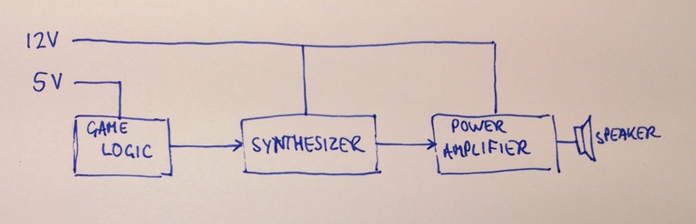
Arcade games typically use two power supplies: 5 volts for their digital circuits, and 12 volts for the sound amplifier. This gave me an idea: how about using the 5 volt supply to run the audio synthesizer, keeping it neatly separate from the amplifier? Clearly the synthesizer wouldn’t just work from 5 volts: I’d already had trouble with it running from about 10 volts in the decoupling experiment. However, there was a solution. It would be possible to boost the 5 volt power supply up to 12 volts using, aptly, a boost converter. Boost converter modules are cheap and readily available thanks to low-cost far eastern manufacturing. The one I chose had a conveniently adjustable output voltage. It didn’t take long to wire it up. I’d already separated the amplifier supply from the synthesizer, and so I just had to take a wire from the existing 5 volt supply to the sound board, check my work and switch on.

zaxxon-power-2

It worked! The sound was now perfect, with no strange thumping effects, and everything seemed to be at the right volume. It remained only to make the modification more solid, and there was even a handy spare hole  to mount the boost converter in. Job done!

wpid-DSC_0326.jpg

Henelec PA25 power amplifier and MU442 power supply

Over on the Vintage Radio Forum, someone asked recently about the Henelec PA25 power amplifier module. The PA25 was produced by Henry’s Radio of London in around 1970. Since I have a pair of them, including the associated MU442 power unit, I’ve documented them here.

Here are a couple of general views. The MU442 has sockets for mains in, signal input (3-pin DIN) and speaker outputs (DIN again). There are also a pair of power supply fuses. Connections to the PA25 modules are via wiring harnesses with edge connectors.

Img_3997

IMG_3999


Here’s what one of the modules looks like. It’s a sandwich of a PCB and heatsink.


IMG_4000


This is what’s on the PCB…


IMG_4003

…and on the heatsink…

IMG_4004


…and the back of the PCB.

IMG_4001


The heatsink has a pretty label on it:

Img_4005


This is the MU442.

Img_4006


Inside, there’s a mains transformer with 2x 22VAC secondary windings, four BYZ13N rectifier diodes in stud-mounted packages, and a pair of smoothing capacitors.

Img_4007


I drew out the schematic diagram of the circuit. It’s made with silicon transistors and is pretty conventional, I think,

PA25_Schematic


Here’s a PDF file of it: PA25_Schematic


150W Boost Converter Schematic

In a recent project, I needed a boost converter to step up 5V to about 8V at a few amps. A few different Chinese-made boost converter modules are available from various sources: I’ve seen them on eBay and Amazon. One very common one is known as the ‘150W Boost Converter’. I believe it’s intended for charging laptops from car batteries. It’s specified to take an input of 10-32V and output 12-35V, which isn’t quite what I was looking for, but the price was right so I thought I’d take a chance. This is what I found.

boost

I had a good look at the circuit board. It’s based on the UC3843 chip, which is a pretty old device (I think it dates back to 1984) and is often found in PC power supplies. However, its age and ubiquity means that documentation on it is readily available. I traced out the circuit, so here’s the schematic diagram:

150W_ boost

You can also have it as a PDF file: 150W_ boost.

It’s a pretty straightforward boost converter topology with a MOSFET switching transistor and a variable resistor in the feedback loop to set the output voltage. There is no over-current, over-voltage or reverse polarity protection at all, and the chip isn’t designed for low power consumption so this module wouldn’t be suitable where very low standby power is a requirement. There are a couple of interesting features, though.

The circuit includes an arrangement with an NPN transistor which feeds some bias to the current sense feedback loop. According to the UC3843 datasheet, this improves the stability of the converter at duty cycles higher than 50%.

The control supply for the UC3843 is derived from a 9V regulator, so it’s independent of the input or output voltage. This is convenient.

The UC3843 is designed to operate from fairly high supply voltages, and won’t start up until its supply voltage reaches 8.4V. That was a bit of a problem for my application, where the input voltage was only 5V. However, there’s nothing to say that the chip power supply has to be the same as the power input. In fact, the module already has a handy 9V regulator which feeds the control chip. Looking at the circuit diagram, there are even a pair of resistors (I’ve labelled them R1 and R2) which select whether that regulator is fed from the input or the output. As supplied, R2 was fitted, so the control chip was fed from the output. Here’s a closeup of the relevant part of the board showing R1 and R2.

DSC_0310crop

My application happened to have a low-current 12V supply available, which would be perfect for powering the UC3843. I simply removed R2 and connected my 12V supply to the point where the black arrow is in the photograph. The boost converter now worked perfectly with a 5V input.

I also had to modify it a little to be able to reduce the output voltage below about 11V. R3, labelled in the photo, is part of the feedback network. I simply removed it and replaced it with a piece of wire. Now the output voltage was variable down to 5V, and I was able to set it to the 8V I wanted.

The module seemed very comfortable delivering 3.3A at around 8V, and drew about 5A from the the 5V input. The heatsinks only got slightly warm.

Unfortunately, the power supply I wanted to run the converter and its load from didn’t like starting up with it all connected. This is quite often a problem with boost converters, since the inrush current at startup can be very large as the controller tries to bring the output up to voltage as quickly as possible. I solved this by adding a soft-start circuit to the module. More on that later.

Espial Arcade Game Pinout

espial

Getting through my collection of not-quite-working arcade PCBs, I’ve just sorted out ‘Espial‘ and made a JAMMA adapter for it. In the process, I discovered something missing from the available pinouts of this game online. In the game you have two weapons: you can drop bombs on ground targets, and fire lasers at flying targets. In MAME, the game uses two separate fire buttons, one for each weapon. However, the published PCB pinouts only show one fire button connection for each player. There’s a DIP switch setting which combines both bombs and lasers on to one fire button, which worked for me, but that’s not the same as having separate control of the weapons.

IMG_3734

I set about looking for the second fire button connections. The MAME source code shows that the second fire button for player 1 is in bit 6 of the port at 0x6081, the same port as some of the DIP switches. The inputs all seem to be handled by 74LS368 buffers. Prodding their inputs with a grounded bit of wire during a game revealed that the second fire button for player 1 was on pin 14 of IC2F. Aha! It does exist. Tracing the PCB tracks led me to pin E on the underside of the edge connector via R17. A similar process led me to pin G for the second fire button for player 2.

Here’s my updated version of the pinout diagram:

              COMPONENT  |  SOLDER
    ---------------------+----------------------
               GND   | 1 | A |   GND 
               GND   | 2 | B |   GND
                     | 3 | C |   
               +5V   | 4 | D |   +5V
                     | 5 | E |   1P.Laser
      Coin Counter   | 6 | F |   
           2P.Down   | 7 | G |   2P.Laser
              Coin   | 8 | H |   
           1P.Bomb   | 9 | I |   Service
          1P.Start   |10 | J |   2P.Start
           1P.Left   |11 | K |   1P.Right
             1P.Up   |12 | L |   2P.Up
           2P.Left   |13 | M |   2P.Right
           2P.Bomb   |14 | N |   1P.Down
               GND   |15 | O |   GND
               Red   |16 | P |   Green
              Blue   |17 | Q |   Sync
                     |18 | R |   Speaker
                     |19 | S |   
              +12V   |20 | T |   +12V
               GND   |21 | U |   GND
               GND   |22 | V |   GND

I also found that it was important to connect up all the power and ground connections, even the seemingly duplicated ones, before the game would start up correctly. But start up it does, and it’s fun. I hope this information is useful to someone.

Img_3737

HP 16500A memory upgrade part 7

In part 6, I established that something was stopping the floppy disc drives in my 16500A working when I changed the ROMs to software version 00.02. Thanks to the help of some on the hp-agilent-equipment Yahoo group, especially Glen Slick, I have determined that there’s an important difference between early CPU boards running 00.00 and later ones running 00.02: the floppy disc controller chip has changed!

The old board has an FDC9793 and the new one a uPD765 (or at least its Zilog equivalent). There are pictures of all the boards here. Now, I started to wonder, could I somehow fit the uPD765 to my board? It seems crazy and would only make sense if it wasn’t possible to exchange the whole board. So I started investigate. As luck would have it I have a functional 16500B with a logic analyzer plugin, so I could have a look and see what was going on around the disc controller on my CPU board. I wired up the relevant pins of the FDC9793.

DSC_0305

Examining the logic analyzer trace, it seems that the CPU is trying to read something from the disc controller, which is at least a start.

DSC_0304

It’s reading from what would be the status register repeatedly, as if waiting for some condition to be true. It gets a value of 0x04 every time, which is presumably not what it wants. It does this at the right stage of the self-test. I thought this was promising, since it is at least addressing the chip. Might it be possible to wire one in place of the other? Their pinouts are different. Comparing them, using their datasheets:

FDC9793 uPD765
1 RESET I active high
2 nWE I nRD I
3 nCS I nWR I
4 nRE I nCS I
5 A0 I D/nS I data/nStatus register select
6 A1 I D0 I/O
7 D0 I/O D1 I/O
8 D1 I/O D2 I/O
9 D2 I/O D3 I/O
10 D3 I/O D4 I/O
11 D4 I/O D5 I/O
12 D5 I/O D6 I/O
13 D6 I/O D7 I/O
14 D7 I/O DRQ O DMA request
15 STEP O Step output nDACK I DMA ack
16 DIRC O Direction (high=in, low=out) TC I end of DMA transfer
17 EARLY O write precompensation IDX I index pulse
18 LATE O write precompensation INT O interrupt output
19 nMR I master reset CLK I 8MHz
20 GND GND
21 +5V WCK I write clock
22 nTEST I tie to +5V RDW I read data window
23 HLT I input, head engaged RDD I read data from data sep
24 CLK I 1MHz in VCO/SYNC O enable VCO
25 RG O read gate to data sep WE O write enable
26 RCLK I read clock from data sep MFM O MFM/FM
27 nRAW READ I raw data from drive HD O head select
28 HLD O head load US1 O unit select
29 TG43 O track greater than 43 US0 O unit select
30 WG O write gate WDA O write data
31 WD O write data PS1 O precompensation shift (early/late/normal)
32 READY I ready PS0 O precompensation shift (early/late/normal)
33 nWF I/O write fault/vfo en to data sep FLT/TR0 I track 0/fault
34 nTR00 I track 0 WP/TS I write protect/two side
35 nIP I index pulse RDY I drive ready
36 nWPRT I write protect HDL O head load
37 nDDEN I double density FR/STP O fault reset/step
38 DRQ data req, open-collector LCT/DIR O low current/direction
39 INTRQ interrupt req, open-collector nRW/SEEK O indicates seek/read/write mode
40 +5V

There are some important differences here. Firstly, the uPD765 expects an 8MHz clock where the FDC9793 used a 1MHz clock. That’s not a good start. The uPD765 includes drive and side select logic, but the FDC9793 doesn’t. The two also differ a lot in how they handle things like write precompensation signals, and the uPD765 effectively multiplexes various signals too.

At this point I think the swap is just too difficult. It becomes cheaper and easier to swap the whole CPU board, if I can find one, or simply upgrade the whole machine to be a 16500B.