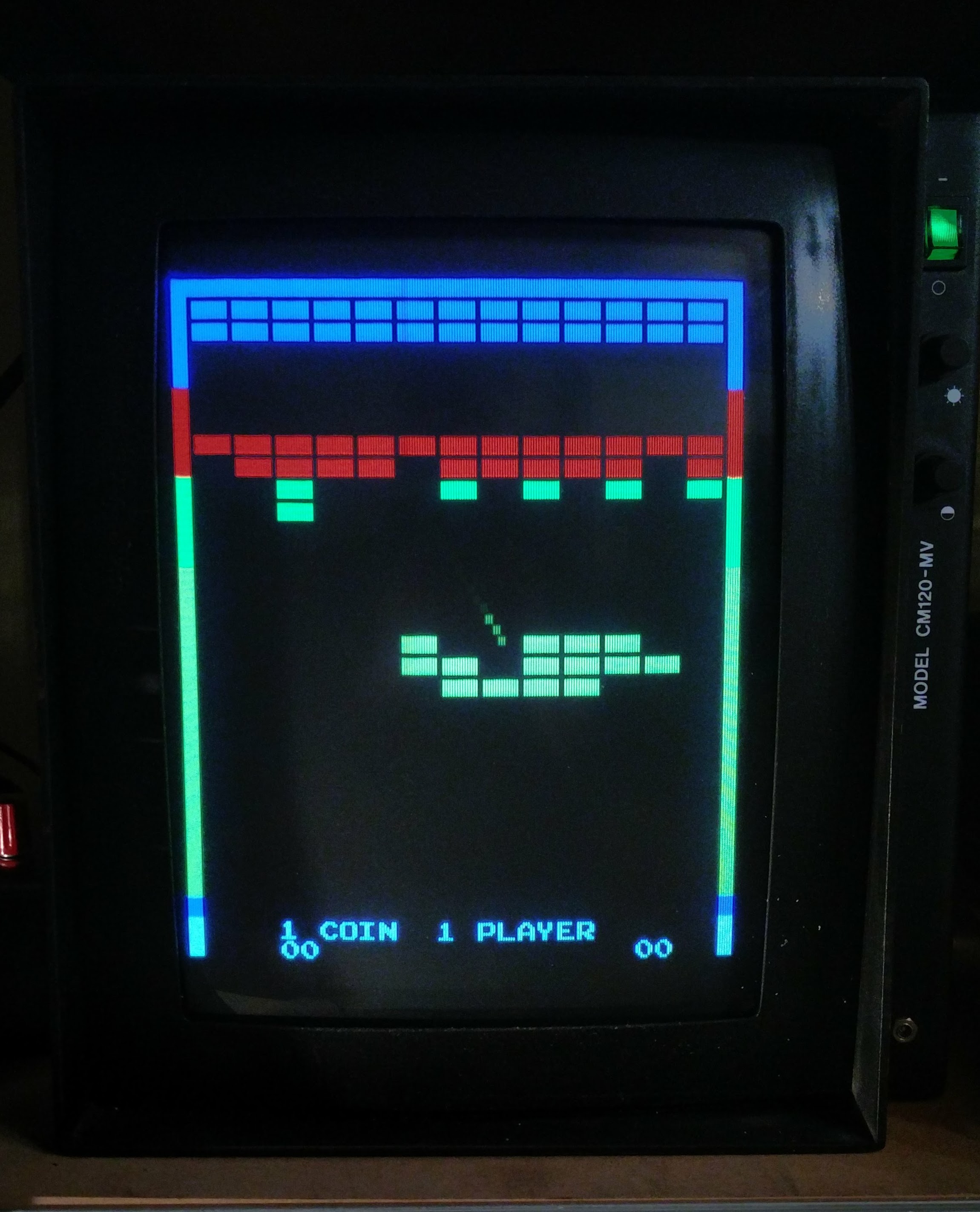
Tag Archives: electronics

Good accuracy from a low cost Real Time Clock

One product I work on has a built-in data logger. This helps us a lot if a problem occurs: we can see the history of any faults. Every log entry is time stamped, which is important. We need to know when it’s been used and how often. However, good timekeeping is a challenge. The product has no Internet connection, it gets stored and moved around a lot, and it’s nobody’s job to check or adjust its clock, so there’s a real problem with clock accuracy.

The real time clock is based on the Microchip MCP7940N chip. The chip uses a standard 32.768kHz crystal for its timekeeping. These crystals are fickle beasts, partly because of the very low-power oscillator in the chip. The oscillator frequency, which is critical for accurate timekeeping, is very dependent on the load capacitance, which itself can vary with different builds of the PCB. The heat of soldering during manufacture also affects the crystal. I’ve seen plenty which have failed altogether, and others whose frequency has shifted significantly. Note the soldering on the crystal’s load capacitors C9 and C10 in the photo below, part of an attempt to find the optimum load capacitance on a prototype board.

img_20180530_100756

All of these issues mean that just assembling the PCB and hoping for the best doesn’t work well. The frequency of an apparently working crystal can be anything up to 100ppm (parts per million) wrong. That doesn’t sound like much, but it works out to nearly an hour’s error per year, which is pretty bad.

Fortunately the MCP7940N has a neat feature which helps a lot. One of its registers, called CAL, holds a value which speeds up or slows down the clock by a small amount, like the regulator on a mechanical clock. But how do we know what the error is, and whether it’s been successfully corrected?

The MCP7940N also has a pin which can output a 1Hz square wave derived from the oscillator. With a sufficiently accurate timer, it’s possible to measure the error in the crystal’s frequency this way.

Checking the correction is more difficult. Because the chip only works on whole oscillator clock cycles, it does the adjustment to the clock’s speed by adding or removing a few clock cycles each minute. It’s therefore necessary to measure the period of exactly 60 of the chip’s seconds to find out how long its minute is, and therefore how accurate the whole clock is.

Getting a sufficiently accurate timer is the first problem. My aim was to get the MCP7940N to be accurate to within 1ppm, or about 30 seconds per year. A useful rule of thumb in metrology is that the measuring instrument needs to be ten times more precise that the quantity being measured, so we need a timer accurate to 0.1ppm, or one part in ten million. To the rescue comes my trusty Hewlett Packard 5335A universal counter. It’s an oldie but a goodie. Mine is fitted with the optional oven-controlled crystal oscillator, an HP 10544A. I checked it and set it up against a Rubidium frequency standard about 8 years ago and it hasn’t been touched since. I checked it this month against the same frequency standard, and it still agrees to within 0.1ppm. Not bad, and certainly good enough for this job.

Measuring the initial clock error is easy enough: connect the counter to the MCP7940N’s 1Hz output and look at the error. The 5335A counter has handy built-in maths functions to make this easier, so it will directly display the difference between its idea of a second and the chip’s attempt.

To measure the corrected clock output over a minute needs a bit more trickery. The 5335A counter has an external ‘arm’ input, and can average a period reading over the length of the ‘arm’ signal. All that’s needed is to arm the counter for 60 seconds and the counter will do the rest. I couldn’t find a way to make the counter do this for itself, so I cheated and used a spare Arduino mini that happened to be lying around. All it had to do was wait for a clock pulse on a GPIO pin, take another GPIO pin high to arm the counter, count 60 clock pulses, then take the arm signal low. Simple.

The test setup looked like this. The scope is there for ease of probing (note the cable from its ‘sig out’ connector to the counter) and it also includes a Tektronix 7D15 timer/counter module connected to the chip’s output. The 7D15 is a lot less accurate (about 1ppm) than the 5335A but it’s good enough to give an idea of what correction is required. The Arduino mini is just about visible at the bottom of the photo.

img_20180427_171833

Here’s a closeup of the scope screen, showing the measured period of the clock’s 1Hz output, 999.9818ms. That’s just over 18ppm too fast.

img_20180427_171723

This the setup screen of the product, showing the 18ppm correction applied to the MCP7940N’s CAL register.

img_20180427_171715

Finally the error in the measured minute, calculated by the 5335A counter gated by the Arduino.

img_20180427_171823

It’s showing that the corrected minute is 301.3 parts per billion, so 0.3ppm, too fast. That’s as good as it’s going to get – about 10 seconds per year. With the clock set up using this process, it has a fighting chance of staying accurate in the real world.

Super Breakout to JAMMA, Part 2: Colour

Having got the power supply working for my original 1978-vintage Atari Super Breakout PCB, it was time to get the screen looking right.

super-breakout-cabinet

At the time Super Breakout was made, video games were mostly black and white. Colour screens were expensive, and so were the relatively complex electronics needed to generate a colour image. But black and white images don’t look too pretty in an arcade, so colour was added by sticking patches of various colours of clear plastic foil on to the screen. Simple, and pretty cheesy, but effective enough to get more coins into the machine. Games like Space Invaders used the same technique.

Fast forward to the 21st century, however, and black and white screens have become rare and expensive while colour screens are standard. My arcade game testing and playing rig uses a colour screen, and I didn’t want to stick coloured plastic on it – it would make other games look very odd! I wondered: how about adding colour to the image electronically?

I had recently been given a MachXO2 pico dev kit from Lattice Semiconductor. It’s a neat little thing, with a 1200-LUT MachXO2 CPLD on it and a built-in USB interface which makes it easy to program. The Lattice Diamond development software is available to download and license at no cost. I wanted to gain experience using this series of chips, since they seem to offer much better price/performance than the older Xilinx CPLDs I’ve used on several projects. Colourising Super Breakout seemed like a neat and vaguely useful example project.

Super Breakout produces a roughly NTSC-standard composite video signal. It’s thoroughly analogue, and there’s no way it could be connected straight to the CPLD. My task was to convert the composite signal into separate sync and video signals, which could then be processed using the CPLD.

atari-monochrome-video-recovery

The industry-standard LM1881 chip separates the sync from the signal. Its output on pin 1 is directly compatible with the CPLD. Getting the video information is a bit more tricky. The video output from the Super Breakout board is about 0.7V peak-to-peak, which isn’t enough to reliably drive any kind of logic gate. I took the easy way out and used an LT1252 video amplifier with a gain of just under 5 to generate a signal large enough to feed into a 74HC132 Schmitt trigger which produces a clean logic output. It was also necessary to add a clamp, the transistor in the top right driven from the blanking output of the LM1881, which forces the black level of the video to a known voltage. Without the clamp, the definitions of ‘white’ and ‘black’ would drift around depending on the picture content, which leads to peculiar black patches and streaks in bright areas of the image.

The resulting waveforms look like this. At the top, the composite video waveform from the Super Breakout PCB. In the centre,  the sync pulse at pin 1 of the LM1881 chip. At the bottom, the digital video ready to feed to the CPLD.

Here’s the circuit built on matrix board, next to the Lattice development board. There’s some more electronics at the bottom left, but more about that in another post.

img_20170215_215403

Generating the colour signal was relatively simple: a counter, clocked at about 6MHz, reset by the horizontal sync signal, indicates the position along each line of video. Some comparisons of that counter with fixed values decide what colour the output should be. A simple AND function of the colour with the video input and – lo and behold – a coloured screen! And no plastic film in sight.

img_20170215_215256


Reliable I2C with a Raspberry Pi and Arduino

There are many ways of connecting sensors and devices to a Raspberry Pi. One of the most popular is the I2C bus. It’s great for devices which don’t need to transfer too much data, like simple sensors and motor controllers, and it’s handy because lots of devices (up to 127, or even more) can be connected to the same pair of wires, which makes life really simple for the experimenter. I’ve mentioned using the I2C bus in another blog post, because sometimes a bit of software fiddling is needed to get it to work.

Recently I’ve been working on a project involving various devices connected to a Raspberry Pi. Some of them use I2C. The project is based around a breakout board I designed for the Multidisciplinary Design Project at Cambridge University Department of Engineering, in which students collaborate in teams to put together a robot. The breakout board is shown next to the Raspberry Pi in the photo below.

IMG_1381

It fits on top of the Pi, and has lots of useful features including a student-proof power supply, real time clock, accelerometer, space for a Zigbee module, analogue inputs, diagnostic LEDs and four motor driving outputs, all wired to convenient connectors.

The analogue inputs and motor outputs are implemented by a PIC microcontroller connected to the I2C bus. The software for the PIC was written by an undergraduate several years ago. It works well, but seems to have some odd habits. I found that it would apparently work, but sometimes an attempt to read data from the PIC would just fail, or return wrong data, and sometimes data would get written to the wrong register. At first I suspected a wiring problem, but examining the SDA and SCL signals with a scope showed nothing wrong. I tested another device on the same bus – a Philips PCF8575 I/O expander – and it worked perfectly every time. That narrowed the problem down to the PIC. Since there was nothing I could do about the PIC’s software, I had to find a workaround.

I spent some time experimenting with where the communications seemed to go wrong. Reading from an I2C device usually involves two separate operations on the bus. The first one tells the I2C device which register address we want to read, and the second does the actual read. The diagram below shows the sequence. The ‘control byte’ in each case sends the address of the I2C device (0x30 in this case) plus a bit indicating read or write.

smbus-transaction

I found a pattern in the failures. From time to time, the write operation which sets the register address would fail, reporting ‘I/O error’. After that, reading the data would return the wrong value. I modified my code so that if the write operation failed, it would retry a couple of times before giving up. It turned out that retrying was always successful, if not on the first attempt then on the second. However, the data read would still return the wrong value. The value returned was always the address of the register I wanted! It seemed as if something was getting stuck somewhere in the I2C system. Whether it was in the Linux drivers, or the PIC software, I don’t know, and I didn’t spend long enough to find out. My assumption is that the PIC software is sometimes just too busy to respond to the I2C operations correctly.

I tried the retry strategy again, and it turned out that the second attempt to read the data byte always got the right value. The algorithm to read reliably looks like this, in pseudo-code:

  if (write_register_address() fails)
    retry up to 3 times;

  read_data();
  if (we had to retry writing register address)
    read_data();

In practice I was using the Linux I2C dev interface to implement this. Yes, it’s a bit of a nasty hacky workaround, but it did get the communications working reliably.

There was another device I wanted to talk to: an Arduino Mini running a very simple sketch to return some sensor data. This also used the I2C bus. There are handy tutorials about how to get an Arduino to behave as an I2C slave device, like this one. The I2C interface is implemented nicely by the Wire library. Implementing a slave involves responding to two events: onReceive and onRequest.

The onReceive event is called when data, like the register address, is written to the slave, and the onRequest event is called when the master wants to read data. My initial code looked like this:

Wire.begin(I2C_ADDRESS)
Wire.onReceive(receiveEvent)
Wire.onRequest(requestEvent)

void receiveEvent(int bytes) {
  registerNumber = Wire.read();
}
void requestEvent() {
  Wire.write(registers[registerNumber];
}

This worked most of the time, but after a few thousand transactions, it would appear to ‘lock up’ and ignore any attempt to change registers – it would always return the same register, and in fact no more onReceive events were ever generated. Of course, it turned out to be my fault. When reading data in the onReceive event code, it turns out to be important to make sure that data is actually available, like this:

void receiveEvent(int bytes) {
  while(Wire.available())
    registerNumber = Wire.read();
}

That solved the problem. It’s annoying that reading non-existent data can lock up the whole I2C interface, so watch out for this one if you’re using an Arduino as an I2C slave.

Lattice FPGA programming adapter from the junk box

Working with Lattice FPGAs recently, I had a need to program one but couldn’t find my ‘proper’ (Chinese clone, bought from eBay) programming adapter. When I started the Diamond Programmer software, though, it claimed it could see a USB programming adapter. It turned out that I’d left an FTDI ‘FT2232H Mini Module‘ attached to the PC. I use the module for all sorts of little debugging exercises: most often as a dual serial port for serial port debugging, but it also works for programming Parallax Propeller microcontrollers.

Img_0603

As luck would have it, the Diamond software recognises the unadulterated FT2232H as a legitimate USB programmer, and pressing the ‘Detect Cable’ button finds it. Note that if you plug in a new USB device, the Diamond Programmer software needs restarting before it can see it.

The FT2232H has two ports, A and B, and these appear as ports FTUSB-0 and FTUSB-1 in the Diamond software. All that remained was to figure out the wiring. Fortunately, there are a lot of clues in the schematics of various Lattice evaluation boards, particularly the MachXO2 Pico Board and the iCE40 Ultra Breakout Board.

diamond-programmer

Here’s the wiring, both for SPI and JTAG, referred to the pins on the Mini Module. I chose to use port B since it was more convenient for my prototype board. Translating the wiring to port A is left as an exercise for the reader.

SPI    JTAG  FT2232H  Mini Module
SO     TDI   DBUS1    CN3-25
SI     TDO   DBUS2    CN3-24
SCK    TCK   DBUS0    CN3-26
SS_B   ISPEN DBUS4    CN3-21
CRESET TRST  DBUS7    CN3-18
GND    GND   GND      CN3-2,4

It works well, and does exactly what it should.

First steps with a Lattice iCE40 FPGA

I’ve just been doing some work with the iCE40 series of FPGAs from Lattice Semiconductor. They’re small FPGAs, with up to 7680 gates, and they’re very low-power, which is nice for mobile applications. From what I can gather, Lattice acquired the designs when they bought a company called SiliconBlue in 2011. I’ve been used to using the Lattice Diamond software with their other chips, but the iCE40 chips aren’t supported by Diamond. Instead, they get their own software called iCEcube2. It’s a bit of a pain to use and not very well documented. I’ve just been through the process of starting a project and getting a very basic design working, and I’m writing about it here in case someone else finds it useful.

Img_0602

The iCEcube2 software looks convincingly like an IDE, but it isn’t, really. It doesn’t even seem to have a way of creating new source code files, and the order in which some things have to be done is not at all obvious. I think iCEcube2 is really designed for taking existing designs and implementing them on the Lattice iCE40 chips. While the software is a complete dog’s breakfast, it does have the key advantage of being free. You do need to create a node-locked licence for it using their licencing page.

iCEcube-blank

To start an empty project, double click Project -> New Project. Select the chip you’re going to use. This creates a folder with the title of the project, containing:

  • <project>_sbt.project
  • <project>_syn.prj
  • folder <project>_Implmnt, containing folder sbt, containing folders constraint, log and outputs. All are empty apart from iceCube0.log in log folder.

Now you can add your source files. If you click on ‘Synthesis Tool’, then an ‘Add Synthesis Files’ menu item appears, but clicking on this doesn’t do anything useful. You have to right-click on ‘Add Synthesis Files’ and select ‘Add Files…’ from the pop-up menu. Go figure. I used a very simple VHDL source file:

LIBRARY ieee;
USE ieee.std_logic_1164.ALL;

ENTITY test IS
 PORT
 (
 d: in std_logic;
 q: out std_logic;
 qn: out std_logic
 );
END test;

ARCHITECTURE rtl OF test IS
BEGIN

 q <= d;
 qn <= not d;
 
END rtl;

At this point I’d expect to be able to allocate signal names (d, q and qn, in this case) to pins on the device package. But you can’t do that yet in the wonderful world of iCEcube2. All the buttons on the toolbar are greyed out. The way to proceed is to double click ‘Run Synplify Pro Synthesis’. Hopefully your code will compile without errors, and lots of files get created.

The project folder now contains:

  • stdout.log and stdout.log.bak
  • synlog.tcl
  • loads of stuff under <project>_Implmnt

Two new files appear in the project under ‘P&R Flow’: <project>.edf and <project>.scf.

Now double-click ‘Run P&R’. The design will get placed and routed, and a bitmap gets generated for programming the chip.

At this point the toolbar buttons for timing constraints, pin constraints, floor planner, package view, power estimator and timing analysis become active. Hurrah! Now you can change your pin constraints.

iCEcube-toolbar-enabled

Click on ‘Pin Constraints Editor’, the fourth icon from the left. Put in the pin locations for the signals you want. Make sure you click the ‘locked’ checkboxes on the left hand side, otherwise the place and route process is likely to move them. Press ctrl-S to save. The constraints get saved in <project>_Implmnt\sbt\constraint\<top design file>_pcf_sbt.pcf. You will then get asked to add the file to the project. Say yes.

If you’re using source control, it’s a good idea to add this file to it. I’m not so sure about all the other junk that iCEcube generates.

Now double-click ‘Run P&R’ again and the new bitmap file will be generated, using your pin constraints.

Programming an actual chip (or at least its SPI Flash ROM) needs the Diamond Programming tool, which comes as part of the Lattice Diamond software and *not* as part of iCEcube2. That’s just another couple of gigabytes to download, and another licence (free) to acquire, so it’s a pain, but it does work.

Servicing a Fluke 12 Multimeter

One of my most-used tools on the workbench is my Fluke ’12’ multimeter. I’ve had it almost 20 years, and it’s my favourite meter because it was clearly designed by someone who had to fix things. It’s rugged, especially in its bright yellow holster, and has so many thoughtful features: it has big buttons and a switch, instead of a rotary knob, so it’s easy to use with one hand. It autoranges quickly and reliably. In continuity and resistance modes, it automatically switches to measuring voltage if it detects one, so you don’t need to worry about changing ranges when debugging things. It doesn’t have fiddly extra features. It doesn’t even have a current range, because it would make no sense: measuring current usually involves breaking a circuit, which you can’t easily do when working on a circuit board. It switches itself off when unused for half an hour or so, saving the battery.

Img_0007

It’s been completely reliable apart from needing a new set of test leads last year (for the first time). However, recently the big, chunky buttons had become reluctant to respond, and needed firmer and firmer presses until they didn’t work at all. That meant I was stuck measuring either DC voltage or continuity. Time to pull it apart and see what’s wrong.

Removing the test leads and holster, then taking out the four screws, reveals the view you get when changing the battery. I’m sure Dave at EEVBlog, master of the multimeter teardown, would approve. Lots of chunky components and very solid construction.

Img_0008

The PCB is held in by the plastic clips at the top and sides. Easing them back lets it and the plastic frame underneath it come out:

Img_0010

The black plastic internal frame (under the PCB in this photo) is marked as being made of polycarbonate, so it’s very strong. None of that high-impact polystyrene rubbish. It’s nice that the membrane for the buttons bears against the frame, not straight against the PCB. This is nice industrial design.

The button membrane is connected by a zebra strip to the PCB. The PCB itself looks nice and clean, and the zebra strip is OK, but the contacts on the membrane look tarnished.

Img_0012

I wanted to test the membrane using the continuity check function of my trusty Fluke 12…oh, hang on, it’s in pieces. Break out the equally trusty Avo 8.

Img_0013

The membrane itself works fine. I cleaned up the contacts using DeoxIT D5 on a piece of paper. I also cleaned all the plastic parts, including the holster, in the office sink with washing-up liquid. Here’s the result, showing resistance mode to prove that the buttons work.

Img_0014

Looking good, working as well as it did when new, and ready for the next 20 years.

Solidlights new LED upgrade

The first Solidlights products to be sold used the Lumileds Luxeon III LEDs, which were state of the art back in 2003. Technology has moved on since then, however, and modern LEDs are much more efficient – they produce a lot more light for the same amount of electricity. Though I’m no longer actively developing Solidlights, I occasionally tinker with upgrades to the ones I use regularly.

For a year or so now I’ve been using a modified Solidlights 1203D dynamo light fitted with Cree XP-G2 LEDs. Getting the best from them requires modifications to the lenses, too, but it’s worth it: the theoretical maximum light output from each LED is 488 lumens, whereas the old Luxeon III could only manage about 80 lumens. I’ve done the modification informally for a couple of customers, too, and they’ve been happy with it.

xpg2

There’s been more interest recently, so I’ve made this upgrade available in the Solidlights on-line shop. It’s listed as part number 99002 under ‘service and repairs’.

Sideways RAM for BBC Micro Model B+

There’s an excellent article by Mark at RetroClinic on adding 32K of Sideways RAM to a BBC Micro with just a couple of track cuts and wires. I’ve performed it on a BBC Model B, in order to replace a Solidisk SWR which never worked reliably even when it was new, and the modification works well. However, I wanted to do it on the BBC B+ I use in the office, and the details are slightly different.

The first thing to note is that the B+’s sideways ROM sockets are conveniently already wired to support 32K chips (27256 EPROMs). There is a row of links to the left of the ROM sockets which select whether each socket is configured for a 16K chip or 32K chip. Each link just selects whether pin 27 (A14 on 27256, /PGM on 2764 and 27128) is tied to +5V or connected to the bottom bit of the ROMSEL register IC45. If the link is to the left, pin 27 is tied high, and if it’s to the right, it’s an address bit. To be honest I can’t see any reason not to leave them all to the right all the time, since pulling /PGM low on 2764 and 27128 chips seems to have no effect other than disabling the chip. However, on my B+ they were all set to the left by default.

The layout of the parts on the board is:

    +------+ +------+ +------+
S19 |      | |      | |      |
S18 | IC62 | | IC68 | | IC71 |
S15 | ROM  | | ROM  | | OS & |
S12 | banks| | banks| | bank |
S11 | 8/9  | | A/B  | | 1/F  |
S9  |      | |      | | BASIC|
    | (S15)| | (S18)| | (S19)|
    +------+ +------+ +------+
    +------+ +------+ +------+
    |      | |      | |      |
    | IC35 | | IC44 | | IC57 |
    | ROM  | | ROM  | | ROM  |
    | banks| | banks| | banks|
    | 2/3  | | 4/5  | | 6/7  |
    |      | |      | |      |
    | (S9) | | (S11)| | (S12)|
    +------+ +------+ +------+

Note that S19 (for IC71) behaves a bit differently. IC71 is always the OS ROM, which is not a sideways ROM, but can be a sideways ROM (in bank 1 or bank F) as well. If S19 is placed to the right, IC71 should have the OS in the top 16K and a sideways ROM image, conventionally BASIC, in the bottom 16K. Which bank this ROM image ends up in depends on the setting of S13. If S13 is set ‘north’, the lower half of IC71 appears in bank 1. If it’s ‘south’, it appears in bank F. Normally bank F is convenient for BASIC.

The key ingredient of the sideways RAM upgrade is to provide a write enable signal to the RAM chip. This isn’t normally present on ROMs because it makes no sense to write to a ROM. The RetroClinic upgrade takes a write signal from IC77 pin 8. This is the write strobe for the uPD7002 ADC and the 8271 floppy disc controller. The corresponding signal still exists in the B+, and is used by the ADC and the 1770 floppy disc controller. It comes from IC27 pin 6, however, which is conveniently close to the ROM sockets.

However, there’s an annoying difference between a 27256 32K EPROM and a 62256 32K RAM. The EPROM has A14 on pin 27, but the RAM has A14 on pin 1 and /WE, the write enable signal, on pin 27.

On the Model B, it’s not hard to cut the tracks to pins 1 and 27 and solder wires on the bottom of the board. However on the B+, the tracks to those pins are on the top of the board, mostly concealed by the socket, and are a royal pain to get to. I could have desoldered the socket, done the modifications and put it back, but that was relatively risky and a lot of effort. I decided to just take pins 1 and 27 of my RAM chip outside the socket and run a wire from pin 27 to IC27 pin 6, and pin 1 to IC45 pin 14 (the source of the address line), on the top of the board. Here’s what it looked like.

DSC_1094

My final discovery was that the Sideways RAM utilities are provided by the 1770 DFS ROM. My B+, however, only had DFS version 2.10, which doesn’t include them. I programmed a ROM with DFS version 2.26, and took the opportunity to shuffle the existing ROMs into 32K chips to save sockets.

This done, the SRAM commands were now available, but the Sideways RAM wouldn’t work. I’d put my RAM chip in socket IC57, which is banks 6 and 7. It seems that the B+ and DFS SRAM utilities only understand about Sideways RAM in the banks which the B+128 would have it: banks 0, 1, C and D, exactly the banks which are not covered by the ROM sockets. Doh!

I needed to move my RAM chip to appear in banks 0 and 1. This was easily accomplished by moving pin 20 outside the socket and soldering a wire from it to IC46 pin 15. IC46 is the address decoder for the ROM sockets, and pin 15 is its /0 output.

Now, when switched on, the machine shows ‘Acorn OS 96K’ (cute!) instead of its previous ‘Acorn OS 64K’, and the *SRLOAD command works to load images into banks 0 and 1.

Img_8121s

In summary, to add 32K of Sideways RAM to a BBC B+ 64K:

  • Move S12 into its right-hand position
  • Bend pins 1, 20 and 27 of a 62256 RAM chip so they fall outside the socket
  • Put the chip with bent pins into socket IC57
  • Solder a wire from pin 1 to IC45 pin 14
  • Solder a wire from pin 20 to IC46 pin 15
  • Solder a wire from pin 27 to IC27 pin 6
  • Make sure your DFS is version 2.26

Now you have Sideways RAM in banks 0 and 1. Job done.

IMG_8120

That syncing feeling: classic arcade games that won’t stay still

I’ve got a collection of classic arcade games from the ‘golden era’ of the early 1980s. They’re not the whole wooden cabinets with flickering lights and cigarette burns, but just the circuit boards from inside. They are easy to store and easy to plug in to a joystick and monitor to play.

However, some of them have always been a bit tricky to see. The monitor I use, a spiffy Microvitec bought surplus from Display Electronics in 1990, has fantastic picture quality but is a bit fussy about its input signal. Specifically, it seems to expect that the sync pulses – the bits of the signal which indicate where lines and pictures start – must conform more-or-less closely to broadcast standards. Unfortunately, the people who designed the old video games weren’t too worried about complying with standards. The result is that, on my monitor, some games tend to flicker and roll, or require very finnicky adjustment of the controls.

There’s loads of information about what video sync pulses are supposed to look like on the web.  This link has plenty of detail. However, the important things here turned out to be that the horizontal sync pulses should be fairly close to 4.7 microseconds long, and the vertical sync pulses should be pretty much three lines, or 192 microseconds, long.

I compared the outputs of various games – one which had never given problems (Mr Do’s Castle) with three which were troublesome (Phoenix, Pleiads and Q*Bert). The results were interesting. Here’s the vertical sync period from Mr Do’s Castle:

mrdocslv

In all the scope pictures, the red trace is the sync output from the game, and the blue line is the vertical sync from my electronics which I’m just using to trigger the scope at the right time.

In this case, the narrow red pulses are the horizontal sync pulses, and the broad area between the dotted lines is the vertical sync pulse. It’s six lines, or about 386 microseconds, wide, which seems to be good enough to keep the monitor happy.

Examining Pleiads and Phoenix, which have the same video electronics, here’s the horizontal sync pulse:

pleiadsh

Oh dear, It’s only 3 microseconds wide when it ought to be 4.7. And the vertical sync pulse?

pleiadsv

It’s a full eight lines wide, or more than 500 microseconds. Those numbers are way off what the monitor is expecting. The result is that the monitor refuses to give a stable picture, which makes playing the game very tricky:

Img_7793

Looking at Q*Bert, its horizontal sync pulses are nearly three times as wide as they should be, at 12.6 microseconds:

qberth

and Q*Bert’s vertical sync pulse looks like this:

qbertf

It lasts more than a millisecond! That’s miles off. The effect on the picture looks like this:

Img_7782

That’s as stable as I could get it. Notice how the left hand side (which is actually the top – the monitor is rotated 90 degrees)  is curved and wobbly. It was fairly hard to adjust the monitor to get the picture stable enough to take a photo.

There are solutions to these problems which involve modifying the game boards themselves, but I didn’t want to do that. I think they’re interesting historical artefacts (even the bootleg ones) and I try to keep them as original as possible. I wanted to fix the sync problems outside the board.

After a bit of experimenting, I came up with a little circuit which regenerates the sync pulses to be a bit more standard.

Img_7778

Untangling the rat’s-nest of wires, the schematic diagram looks like this:

syncfix-schematic

The circuit is simple and cheap, using two standard TTL logic ICs. It ought to work with 74HC series chips as well, but some of the resistor values might need changing. The diode is any common-or-garden signal diode: a 1N4148 or 1N914 is fine. It works like this.

  • IC1B is a monostable which triggers on every sync pulse, generating a pulse 4.7 microseconds long. These become the new horizontal sync pulses.
  • IC2B combined with D1, R3 and C3 form a sync separator which triggers the monostable in IC1C only on sync pulses which are longer than about 40 microseconds.
  • IC1C is a monostable which generates vertical sync pulses about 200 microseconds long.
  • IC2E combines the new horizontal and vertical sync pulses into a new sync signal.

The output isn’t what you might call broadcast standard, but it’s close enough to make the monitor happy. I’ve tried it on a few games and it works even on games which the monitor was happy with before. Here’s the results from Pleiads:

pleiadsc

Nice horizontal sync pulses, with a vertical pulse 193 microseconds long. There are a few extra pulses around but the monitor doesn’t seem to mind.

Img_7783

The results from Q*Bert are also good, though the vertical sync looks even more odd:

qbertc

The vertical sync pulse is a sensible length, but there’s a long pause after it before the horizontal pulses start again. That doesn’t bother the monitor, though, and all the wobbles have gone away. Here’s the test setup in use.

Img_7777Sorry about the mess, but at least the display on the monitor is tidy. Mission accomplished.

Parameters in Altium Designer

I use Altium Designer a lot for schematic capture and PCB layout: drawing electronic circuits, in other words. It has a handy feature called ‘Parameters’ which should make it easy to add a piece of data, for example a version number or the author’s name, to a project and have it appear on all of the documents which form part of that project. I’ve always had trouble getting it to work, but I’ve finally cracked it and I’m writing down my findings here so that I don’t forget them. Other people may find it useful too.

V1_0

1. It’s possible to set parameters on a project and then refer to them in documents, but if there is a parameter in the document with the same name, it will hide the project parameter.

For example, all schematic documents have a ‘Revision’ parameter by default. If I set a ‘Revision’ parameter for the project, it won’t appear in any of the documents because the document ‘Revision’ parameter hides it. If I choose a new name which isn’t already used in the documents, like ‘ProjectRevision’, it does appear in the document.

2. In schematic documents, parameters are referred to using the equal sign:

=ProjectRevision

In PCB documents, they’re referred to using a dot:

.ProjectRevision

It’s bonkers, but it’s true.

Here’s my recipe for getting a version number to appear on both schematic documents and the PCB layout.

  1. Set your version number on the project using Project -> Project Options -> Parameters. Call it something which isn’t one of the default document parameters. I use ProjectRevision.
  2. In schematic sheets, use =ProjectRevision in text strings to call up the version number.
  3. In PCB sheets, use .ProjectRevision in text strings to show the version number.
  4. Make sure ‘Convert Special Strings’ is switched on in both schematic and PCB editors otherwise you won’t see the version number.

For the schematic editor, select Tools -> Preferences -> Schematic -> Graphical Editing and make sure ‘Convert Special Strings’ is ticked.

For the PCB editor, select Design -> Board Layers and Colours -> View Options and make sure ‘Convert Special Strings’ is ticked.

That’s it. Using parameters has made managing my Altium projects quicker and easier.