Category Archives: Uncategorized

Windows 10 Boot Problems: error 0xc000000e

Monday morning. Arrive at the office with lots to do. Switch on the computer, and…

IMG_20190129_104214

That’s not what I wanted to see. There’s lots of advice out there on the web about fixing this problem, but it turned out not to be so straightforward.

The first step was to get hold of a bootable Windows 10 installer. That entailed installing a desktop and web browser on my office Debian Linux machine which normally runs withou a monitor. Downloading the image from Microsoft was easy enough, though it’s 4.5GB in size so takes a while. I wrote it to a USB stick (which I had to go and buy, of course) and…nothing. It turns out that the Windows 10 .iso image is only suitable for writing to a DVD, and is not a ‘hybrid’ image which can work also on a USB stick. Of course, I didn’t have any blank DVDs lying around, did I?

Luckily Linux was able to mount the .iso image so I could see the files inside it. That meant it was possible to reformat the USB stick, creating a single partition formatted FAT32, and copy the files on to it.

IMG_20190128_151537

This ran in to a problem because the main archive of Windows files, /sources/install.wim, is just over 4GB in size and thus can’t be written to a FAT32 filesystem in its entirety. I tried to fix this by formatting the stick in ExFAT or NTFS, but my PC’s motherboard (an Asus Z77-Wifi) can’t boot from those filesystems so that didn’t get anywhere. I suspect the right answer is to use UEFI boot, creating a FAT32 partition with the EFI folder on it, and a separate NTFS partition with the other files on. But I was in too much of a hurry for that and decided to just put up with a slightly truncated install.wim file.

Now I had a bootable Windows 10 recovery/install USB stick. Great! The advice from Microsoft is to use the ‘fix startup problems’ option available on the menu. So I did that, and it spent a while diagnosing, then proclaimed that it couldn’t fix my PC. Great. I tried the other options (returning to a system restore point, removing the latest updates) but they all denied that my PC had Windows 10 on it at all.

This is getting annoying. Time to break out the command line, which is probably the most useful tool in the Windows 10 recovery toolkit. The official advice from Microsoft is to do this:

bootrec /scanos
bootrec /rebuildbcd
bootrec /fixmbr
bootrec /fixboot

But the /rebuildbcd stage failed for me, with a ‘The requested system device cannot be found’ error. The next advice I found was to manually reconstruct the BCD (the Boot Configuration Data, which tells the boot process where to find the operating system) by doing:

bcdboot c:\windows

But that didn’t work either.

IMG_20190128_172005

I had to dig deeper. Luckily I’m not the only person to have had this problem. This page at screwloose.com.au explained more advanced use of bcdboot, in which it’s possible to tell the tool where the Windows installation lives, and where the System partition which holds the boot information is. I had to rummage round with diskpart to find the right drive letters, because the layout of the partitions on my drive meant that they were not the same as during normal operation. However, I came up with the following:

bcdboot e:\windows /l en-gb /s g: /f all

which worked! It completed successfully! Reboot and…the error was still there. Looking more deeply with diskpart, it turned out that the 100MB partition (drive G:) that was supposed to be the startup partition was formatted NTFS and wasn’t marked as active. The screwloose page indicates that the startup partition needs to be formatted as FAT32 and marked as active. Clearly, formatting it FAT32 deleted all the data on it, so I ran the bcdboot command again to re-create it.

Success! After a shutdown, the PC booted and came up as if nothing had happened. I’m happy that it’s working again, but it’s still a mystery how the error occurred. Something must have got corrupted, but I can’t believe that the entire contents of the startup partition got erased and replaced with an NTFS filesystem.


Hacking child barriers

This post contains no electronics or software, just woodwork.

Our house is full of traps for the inquisitive toddler. There’s cat food and litter, an office full of sharp tools, a fireplace, and most tricky of all, a staircase descending from the corner of the living room guarded only by a coffee-table-height shelf.

Fortunately, there is a handy range of wooden barriers available from various sellers on allegro.pl (search for ‘bramka’ or ‘barierka’ to get started). It’s a sort of modular barrier system, with a basic unit 91cm wide, though other widths are available. The sections screw together with plastic couplings that allow them to hinge. Wall mounting brackets and feet are available, as are sections with a child-proof gate built in. They’re cheap and simple enough that hacking them for specific jobs is easy and worthwhile.

Here’s a set across the end of the living room, protecting the fireplace and cat flap to the garden. These are almost freestanding, but tied to the bannisters at one end with string and blu-tacked to the floor by the window.

IMG_20180311_144905.jpg

The steps up to the office are guarded by these two sections. I added the cat flap in one of them so that the cats can get to their food and litter tray.

IMG_20180318_152052.jpg

The stairs down from the living room are guarded by another hacked set of barriers, cut to length and with an aperture provided for our eldest son’s favourite bookshelves.

IMG_20180311_144822.jpg

I used the leftover upper and lower rails from the segment I’d cut down in length to make a rail to hold the ends of the uprights above the bookshelves. There’s a join in the middle done with one of the plastic hinge pieces and a not inconsiderable amount of wood glue.

The barrier is held up using zip ties through plastic corner blocks screwed to the underside of the wooden shelf top, so the screw holes won’t show when we eventually remove it. Felt pads on its feet stop it scratching the wooden floor.

RIAA phono preamp for Tascam M-1B Line Mixer

In the workshop I have a couple of these Tascam M-1B line mixers. They’re a very useful box: they have eight inputs, each with a level control and pan pot, which are mixed together and fed into a master volume control. There’s also a pair of headphone outputs with their own volume control driven by a headphone amplifier with enough voltage swing to drive 600 ohm headphones properly. Into the mixer I typically feed the sound output of my PC, other audio sources such as a cassette player (yes!), and a spare cable lying around on the workbench ready to connect to whatever I’m working on, or my phone. The output is connected to the workshop speakers. With this setup I can hear all the sources at once without fiddling around, switching anything or unplugging anything.

IMG_0608.jpg

Tascam M-1B Line Mixer

The workshop I set up a couple of years ago turned out to have space for a new audio source: a turntable. Great! I can listen to vinyl (not ‘vinyls’, please). I had a spare turntable on the shelf, so I put it in place. The trouble is, the turntable has a magnetic cartridge which can’t be connected straight to the line inputs on my trusty mixer. It needed amplification and RIAA equalisation. I could have just gone and bought an off-the-shelf preamplifier, but where’s the fun in that? Looking at the back of the Tascam mixer, there’s a blanking plate which looks perfect for adding a preamplifier, neatly built in. No worries about trailing cables or yet another power supply to plug in. Now to find a suitable circuit.

IMG_0609.jpg

A quick web search pulled up an application note from National Semiconductor for their LM833 audio op-amp which shows a simple preamplifier circuit. It then goes on to describes the circuit’s deficiencies and how a two-stage design can improve on it, but I decided to stick with the simple version.

I didn’t have any LM833 op-amps in the spares box, but did have some NE5532s, which are not only an excellent audio op-amp but live two to a package. Finding the passive components in the spares box also proved to be a challenge. Getting the right component values is one thing, but finding two identical ones of each proved to be impossible. However, all was not lost, so I thought. The RIAA equalisation curve needs three time constants, of 75µs, 318µs and 3180µs. I found pairs of resistors and capacitors that gave the same time constants as R1C1 and R2C2 even if their values weren’t what the original design specified. Here’s a circuit diagram with my substitutions marked in red.

riaa-schematic-modded

I built up a small piece of matrix board and tried it out. It worked, but didn’t sound quite right: there was a noticeable lack of bass. I decided to check the frequency response. The application note shows a useful table of the RIAA response at various spot frequencies, so I had something to compare my results with. I used the ARTA STEPS program with a PC sound card to measure the frequency response of my circuit. It took a bit of fiddling with the levels to get good results, since the phono preamplifier has a lot of gain, but the result looked like this.

response-first-attempt

The curve looks convincingly like the RIAA curve, but it should be +17dB at 50Hz (relative to 1kHz). In fact it’s more like +13dB in my version, so I’ve lost 4dB of bass. At the other end of the spectrum it’s more accurate: at 20kHz it’s at almost exactly -20dB as it should be. (Note, when taking readings from the plot, that the level at 1kHz is about -3dB. It’s the relative levels that are important).

What I’d neglected in my component value calculations was that the relative values of the two RC networks are also important. The National Semiconductor application note actually goes on to explain more about this, but I hadn’t read any further than the circuit diagram. Rather than delving in to the maths and risking discovering that I needed more components I didn’t have, I started playing with the values I actually did have. Here’s a plot of the before-and-after empirical results.

response-first-and-second-attempt

The green curve is the modified version. The level at 50Hz is now +17dB relative to the level at 1kHz, as it should be. Below 50Hz there’s a bit of a rolloff, but that’s not something I’m worried about – my speakers don’t go down that low and it makes for a useful rumble filter. The modified circuit is shown here.

riaa-schematic-modded-v2

I had to change both RC networks to get a good result. The time constant of one of them (11k/6n8) is still 75µs, but the other (180k/22n) is more like 4000µs than 3180µs. I suspect it’s interacting with the time constant of R0C0 to give roughly the right result.

IMG_0616.jpg

It fits neatly in to the slot in the back panel of the mixer. The toggle switch connects the output of the preamplifier to inputs 1 and 2. Switching it off leaves those inputs available for normal line-level use if desired. There’s also an earth terminal.

IMG_0617.jpg

Time for some testing. What were the skies like when you were young?

IMG_0621.jpg

Canon S100 Shutter Button Fix

This is my Canon S100 digital camera. After long, somewhat arduous service, the shutter button started playing up: it would focus but not take the photo. Eventually I got a mobile phone with a better camera and quietly forgot about the Canon. The S100 has been extensively frozen, boiled, soaked, rattled and trodden on, so I figured that the shutter button problem was just due to the abuse. It doesn’t owe me anything. However, it’s still useful for some things the phone camera won’t do: it fits a tripod, and has good long exposure and manual control facilities including a handy neutral density filter.

IMG_20180204_165606.jpg

Trying to use it to take some tricky oscilloscope photos the other day, the shutter button got really annoying. I searched on line for the problem and discovered that it’s quite common. That sounded like an interesting problem to me. Here’s my attempt at fixing it.

Before we start, don’t try this unless you’re used to dealing with annoyingly tiny things and have the tools to match: jeweller’s screwdrivers, tweezers, a very fine soldering iron and either amazing close-up vision or a good magnifier.

The camera comes apart surprisingly easily. There are six little black screws on the outside: two on each end and two on the bottom, close to the tripod mount. Take those screws out. The back comes off very easily – take care not to lose any of the buttons though.

IMG_20180204_165751.jpg

The front also comes off easily, though there’s a little FFC connector to the setting ring round the lens. Unplug it carefully. It doesn’t have a locking bar so the flex PCB just pushes in and out. There’s also a foam gasket round the lens and the plastic cover for the HDMI and USB sockets. They’ll fall on the floor.

IMG_20180204_165854.jpg

The shutter button and other controls are underneath the top cover. There are two more screws to remove: one on the front near the lens and one on one end. They’re different lengths so take note of where each came from. Before removing the top, there’s one more FFC to unplug. This one connects to the microphones. Again it has no locking bar so just pull gently. It’s the middle of the three FFCs in this photo.

IMG_20180204_170148.jpg

With the top cover off, the controls themselves are revealed. On the left here, the function selector rotary switch, then the shutter button and zoom switch, then the power button, and on the right the big square thing is the GPS antenna.

IMG_20180204_170233.jpg

If you put the battery back in, the camera actually works fine in this dismantled state, so it’s easy to try experiments. I prodded and poked the shutter button. Sometimes it worked, sometimes it didn’t. I doused the button with my favourite contact cleaner (DeoxIT D5) to no avail. I looked on the web for replacement buttons: “double action tactile switch” seemed to be the best thing to search for. There are lots out there which might fit, but they’d take a while to get hold of and would be really fiddly to solder, especially with the zoom switch so close by.

I wondered about a mechanical solution, extending the plastic rod from the outside shutter button that presses the switch to give it more poke, but sometimes the switch just refused to work no matter how hard I prodded it with a screwdriver, so that probably wasn’t worthwhile.

Given that it wasn’t worth spending a lot of time on what’s effectively a life-expired camera, an alternative engineering solution was called for. The first stage of the shutter button, the half-press to lock the focus and exposure, still works reliably. What if I just wired it in parallel with the shutter release contact? Then there would be no way to lock the exposure and focus, but at least the camera would take photos.

Some fiddly soldering with a fine iron bit and some polyurethane-insulated mod wire later, the two opposite corner contacts on the button are connected…

IMG_20180204_172823.jpg

…and the S100 lives again. It’s not a full fix, call it a workaround, hack or bodge, but it’s good enough for me to take pictures. Oh yes, and assembly, as somebody once said, is the reverse of disassembly.

Replacing the screen of a Wileyfox Swift phone

For the last couple of years, my wife has been using a Wileyfox Swift phone. For a budget smartphone, it’s had a few niggles but has generally been very good. A few weeks ago we and the phone got caught in an almighty rainstorm and the phone got wet. Leaving it to dry overnight didn’t help: it just made a funny fizzing noise when we put the battery back in.

I took it apart and discovered that water had got trapped in various places, not least the internal connectors to the display, cameras and so on. Some tracks on the display ribbon had completely corroded away overnight! Lesson one: if a phone gets wet, take it apart to dry it out properly. Don’t wait and see what happens.

IMG_20171007_213923.jpg

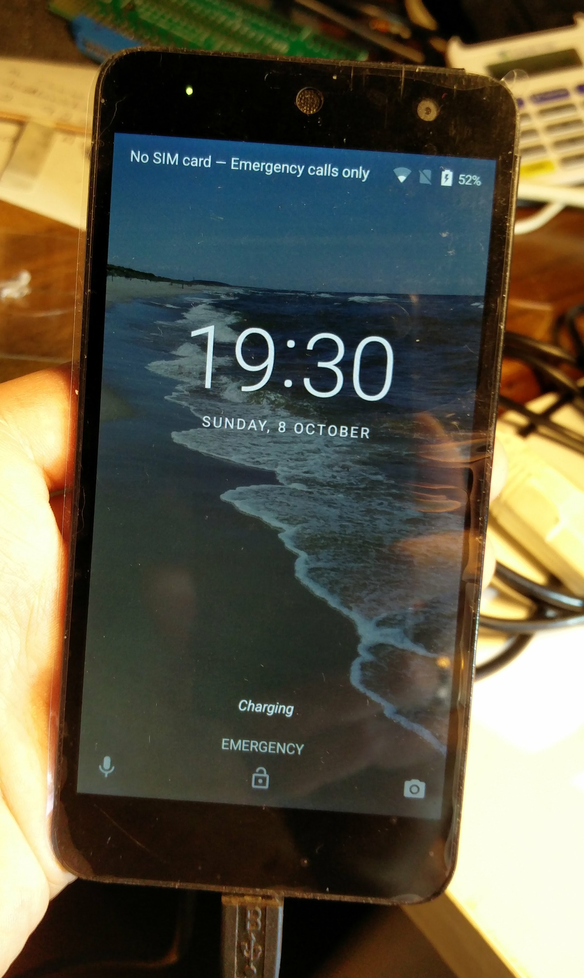
I dried out everything else with warm air and tried the phone again. It seemed to work, giving a little vibrate when I switched it on and showing the charging LED correctly. But there was nothing on the screen. Since the damage to the display connector was plain to see and nothing else seemed to be wrong, I thought I’d try changing the screen.

A replacement screen was only £25 from a Chinese supplier on eBay. It arrived quickly, very well packed with a dinky little bag of tools too, but absolutely no instructions. I couldn’t find any on the web, either. Lots of stories about Wileyfox’s screen replacement policy, but no description from anyone who’d actually done it. Well, here’s how I did it. Or, more precisely, how I’d do it again next time – I did the dismantling in the wrong order which made it unnecessarily difficult. Many of these photos were actually taken while I was reassembling the phone.

First, unclip the back of the phone in the usual way as if to change the battery or SIM card.

IMG_20171008_193146.jpg

Take out the battery and undo all the little screws which hold the inner case on. I think there are nine of them and one of them is behind a sealing sticker. Use a spudger or fingernail to gently unclip the inner case from the phone’s frame, and the insides will be revealed. Notice here the red spotty sticker – a tell-tale that the phone has been wet.

IMG_20171008_192819.jpg

This much dismantling is enough to see whether the phone will work with the new screen. The screen connector is at the top left, labelled ‘BY’ in the photo. Flip up the brown tab with a fingernail and the flexible PCB will come out. It’s easy enough, though a bit fiddly, to plug in the replacement screen, wedge the battery in place and switch on.

IMG_20171007_214101.jpg

Joy! It works. The repair is worth continuing with. Now, remove the battery and gently unclip the black plastic assembly at the bottom right.

IMG_20171008_192756.jpg

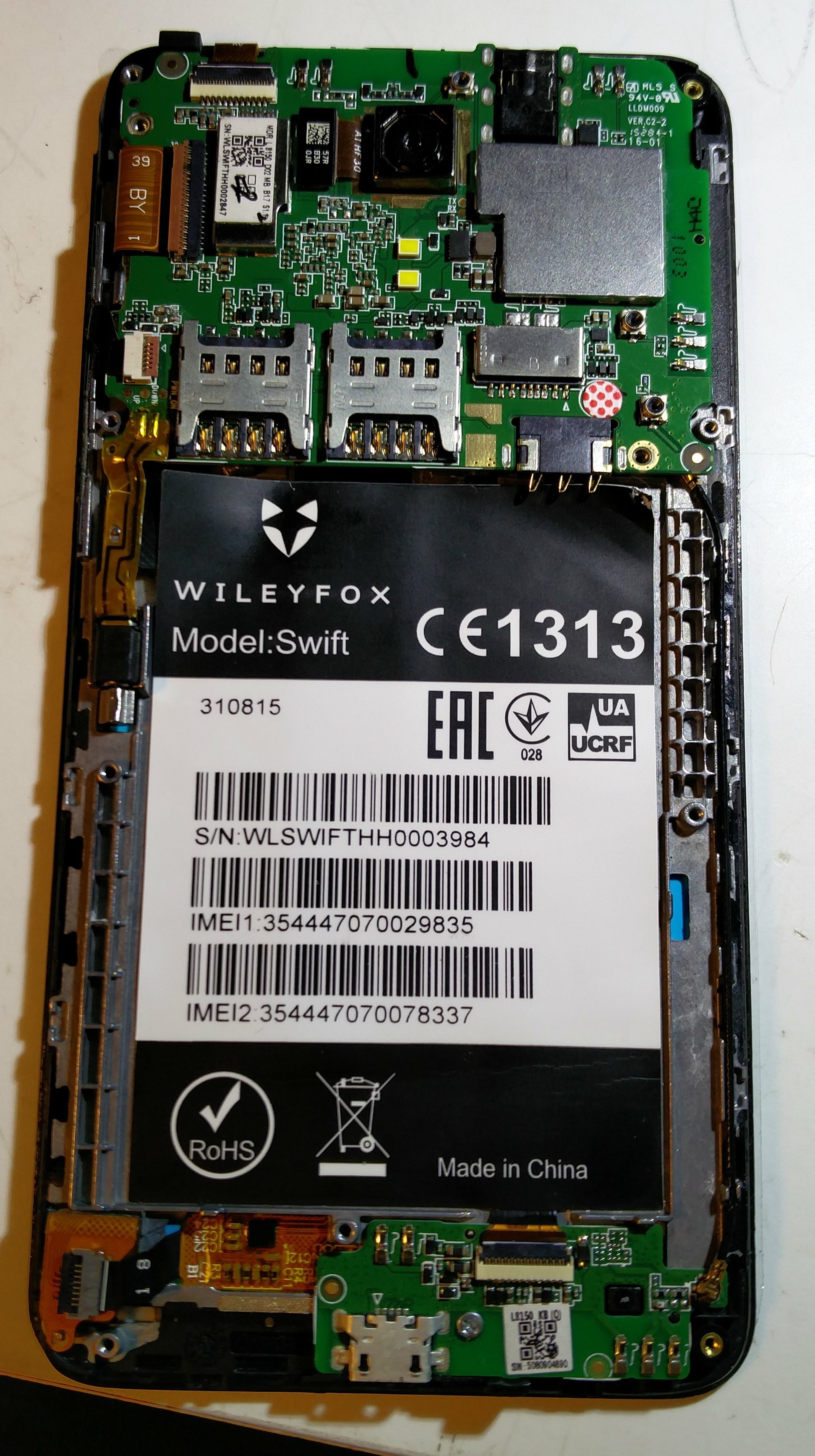
The whole phone is a miracle of industrial design and packaging, but the way the display is fitted is kind of awkward. It has a flex PCB which goes all the way from the bottom of the display up the inside of the phone to the motherboard connector, and runs behind the big identification sticker. Even more odd is the arrangement in the bottom left hand corner: a chip which I believe is the touchscreen controller sticks up on a bit of flex PCB through a hole in the phone’s frame, folds back on itself and has another connector which connects it to another part of the display flex PCB, so the whole thing forms a kind of knot around the frame.

To remove the screen successfully, it’s easiest to remove the motherboard first. There are various connectors to remove:

  • display connector at top left, if you haven’t already done it
  • selfie camera connector also at top left (flip up the black tab)
  • another connector with a white flip-up tab by the SIM sockets

Remove the two screws holding the PCB and gently unclip it – it has clips on the left and right edges. Now there are two connectors to remove from the underside of the board:

  • tiny ribbon plug which goes to the USB socket. This will probably just drop off itself, but it’s really fiddly to put back.
  • U.FL-type antenna connector on the right hand size. Carefully prise it off with fingernails or tweezers.

The vibrator motor is attached by soldered connections on another flex PCB. I left it attached, but it might be possible to unclip it from the frame or desolder the connections. Be careful, it’s fragile.

IMG_20171008_192208.jpg

Note how the screen flex PCB  goes underneath the sticker. It turns out that it also runs underneath the USB flex PCB. Peel off the sticker (a bit of gentle heat helps to soften the glue) and peel back the USB flex PCB. I had to score the screening tape between the two flexes.

IMG_20171007_223816.jpg

Now the screen flex PCB is free all the way to its hole through the frame near the bottom of the sticker.

Now to untangle the fiddly bit at the bottom left. First, unplug the little connector by easing up the black tab. Mine also had a bit of yellow Kapton tape holding it down. Withdraw the flex PCB from the connector and straighten out the folded flex PCB with the chip and connector on it – it’s held in place by sitting on a little peg on the frame.

IMG_20171007_224111.jpg

Now the screen is fully disconnected. Time to remove it from the front of the phone.

The screen is bonded to the Gorilla Glass sheet which forms the front face and touchscreen. This in turn is just stuck to the phone’s frame with double-sided tape. I used a heat gun to warm the glass and soften the adhesive, and a combination of a Stanley knife and spudger to ease it away from the frame. The glass is surprisingly strong and flexible: I managed not to break it.

IMG_20171007_221326.jpg

IMG_20171007_222156.jpg

Once the tape has all softened and come off, the screen’s flex PCBs should come free with a bit of wriggling. Now clean off the self-adhesive goo. I used a spudger and car brake cleaner for this. The surfaces of the frame should be clean and smooth ready to accept the new screen.IMG_20171008_112802.jpg

The new screen needs a bit of preparation before fitting. The little connector for the touchscreen has to be disconnected:

IMG_20171008_113242.jpg

and it needs some self-adhesive tape applying, because it doesn’t appear to come supplied with any. I used little bits of carpet tape (!), shown in the photo below still with its yellow backing paper on.

IMG_20171008_191605.jpg

Now thread the screen’s flex PCBs through the holes in the frame where they should fit, being particularly careful with the folding chip thingy, and the touchscreen ribbon which is easy to get trapped and forget about. Once you’re happy that the flex PCBs are sitting in the right places, peel off the backing from your double-sided tape with a scalpel or tweezers and stick the screen in place.

Assembly is the reverse of disassembly, to coin a phrase.

Dress the flex PCBs into their final positions. Fold up the touchscreen chip and connector and pop it on to its little peg, then plug in its ribbon and lock the connector. Then lay the flex PCB to the motherboard in place, lay the USB flex PCB on top of it and re-stick the Wileyfox sticker. Don’t get cat hair on the back of the sticker because it won’t stick properly.

Put the motherboard back in, taking care to reconnect all the cables including the really fiddly one to the USB flex PCB. I found I had to manipulate it with the blade of a knife underneath the motherboard. Once the screen is reconnected, it’s time to switch on for a test.

IMG_20171008_192925.jpg

Success! Now just to put the screws back in and celebrate. The phone works again, though the rear-facing camera appears to have died. I don’t know if that’s because of the water or because I dislodged its connector and didn’t notice. One day I’ll have another look at it. Until then, this phone is now only a spare, so nobody’s too bothered about not being able to take photos with it.

IMG_20171008_193036.jpg

Repairing the display of a CAP reader

My bank in the UK requires me to use a CAP reader for some online transactions, its security compromises notwithstanding. It’s quite simple to use: I slide the bank’s card in to the slot and follow the instructions on the display and on the bank’s web site. At the end of the process it displays a number which I have to type in to the web site in order to authenticate the transaction.

The problem is, over the last few years, the displays have been gradually failing and losing rows and columns of pixels. It reached the point this morning where I couldn’t read the numbers on either of the CAP readers I’ve got, and so I couldn’t make a payment to a supplier. Getting hold of a replacement reader would take a while – I’m outside the UK at the moment – so it was time to see if they were repairable.

IMG_20170927_103354

Some of the fixing screws are hidden. There’s one underneath the label in the centre (which displays ‘void’ when it’s peeled off – never mind), two under the feet, and four inside the battery compartment, which itself is closed with one little screw.

IMG_20170927_103837

The case unclips, and then there are two black plastic pieces which form the card slot. They’re held by another six screws. That removed, we can see the PCB and display. The display is connected by a ribbon which is bonded to the PCB using a special conductive adhesive. The adhesive appears to gradually come unstuck, so the display stops working. Squeezing it with a fingernail restores some missing parts of the display temporarily.

IMG_20170927_103238

There are lots of guides on the web about repairing these things and I’d had a few unsuccessful attempts previously on other gadgets. This time I was successful, and the method I used was simple. Lay a piece of paper over the area where the ribbon is stuck to the PCB, and then apply gentle pressure with a hot soldering iron to melt the adhesive. I worked my way along in a series of squeezy dabs. The paper chars a bit, but that’s just an indication that it’s working.

Having done the whole ribbon, carefully peel off the paper. It tends to stick to the ribbon so pull it off gently so as not to pull the ribbon off the PCB.

IMG_20170927_103301

Success! The display is working again, tested using a bench power supply clipped on to the battery contacts. I tickled the leaf switch which indicates that a card is in the slot. Of course the card is not responding – it’s not there.

IMG_20170927_103331

I did both the readers I’ve got, and they both worked. I then tried an actual banking transaction which also worked, so there’s no funny security boobytrapping going on. That’s good for me, because I can repair my CAP readers, but less good for anyone who doesn’t know where their CAP reader has been.

IMG_20170927_104626

Tektronix 7A18 versus Soviet Я4C-90

In a previous article, I described briefly the Tektronix 7000 series of oscilloscopes and some that looked awfully similar from the Soviet Union. Having the technical documentation from both, I decided to do a comparison and see what, if anything, the designs owed to each other, bearing in mind that the soviet version appeared at least 7 years after the US one.

I chose the vertical amplifier plugin for comparison. The soviet one is called the Я4C-90, and looking at its specifications (2 channel, about 100MHz bandwidth) it seems very similar to the Tektronix 7A18. Here are the two side by side: my own 7A18 on the left, and a picture of an Я4C-90 from the internet on the right.

7a18-r4c90

They have a lot in common. Where Tek have used rotary switches for the trigger source and display mode, and a slide switch for the channel 2 polarity, the USSR used pushbuttons for those functions. In addition, the Я4C-90 has a 20MHz bandwidth limiting switch, like the (200MHz bandwidth) Tektronix 7A26.

I’ve cut-and-pasted sections from each of their technical documentation in order to be able to compare the designs. Let’s start at the front end: the attenuator.

Attenuator

tek7a18-attenuator

First, Tektronix. They have used x100, x10, x4 and x2 attenuators with switches arranged to bring them in to circuit for the various deflection settings, from 5mV/div to 5V/div.

r4c90-attenuator

Now the USSR. They have used x100, x10, x4 and x2 attenuators with switches arranged…oh, hang on, it’s exactly the same. Even the switch combinations are the same. And whoever drew the diagram had exactly the same idea as the Tektronix drawing office when it came to representing the switching.

Well, let’s move on to the main amplifier.

Amplifier

tek7a18amplifier

Tektronix have used a FET input stage followed by a couple of bipolar differential gain stages, with an emitter follower on the output. And the USSR? Well, the input stage is visible on the right hand side of the attenuator diagram, and it’s practically identical to the Tek one even down to some of the resistor values. They didn’t have Tek’s matched dual FETs so had to make do with two individual ones matched on test. Let’s look at the rest of the stages.

r4c90-amplifier

Oh look! Two differential bipolar gain stages, just like Tek. I can only see two noteworthy differences: the gain control acts after the second stage rather than after the first, and the USSR version doesn’t have the emitter follower on the output.

Next comes the channel switch, which selects between channel 1 and channel 2 to feed to the mainframe.

Channel switch

tek7a18-channelswitch

To get high performance here, Tektronix actually designed and made their own ICs. The channel switch, U270 in the diagram, uses a 155-0022, which appears in all sorts of places in Tek equipment where switching or addition of differential signals is needed. That’s followed by a transistor stage, Q280/Q380, which drives the mainframe. Here’s the soviet equivalent.

r4c90-channelswitch

Fancy that. There’s a special module, MC1, which does the switching. An internal circuit diagram  is also present, which looks suspiciously similar to the rather ambiguous diagram of the Tek 155-0022 chip. The soviet module is actually a 04КН009, which has been extensively reverse engineered by Erik Baigar, see his site here. Interestingly it’s a hybrid module rather than an integrated circuit, though it clearly does the same job.

Interesting here is the frequency compensation network. The Tek design has, between pins 1 and 16 of U270, a couple of RC networks, with one adjustment to get the high-frequency response of the stage right. Conventional enough.

The USSR design has a whole load more stuff in the same position, between pins 1 and 14 of MC1. In addition to three RC time constants with three adjustments (!) there’s a curious arrangement involving a thermistor R4 and a pair of varicap diodes D1 and D2, which seems to do some temperature-sensitive frequency response adjustment. It could be very creative design, but it smacks of desperation to me: the 04КН009 module is probably more sensitive to temperature variations than the Tek chip.

Bandwidth limiting

The final transistor stage before the output isn’t shown on the USSR diagram. It has a separate page to itself. It’s a little more complex than the Tektronix 7A18 because it has the 20MHz bandwidth limiting function. Now, there’s a Tek plugin, the 7A26, which has a 20MHz bandwidth limiting function. Just for fun, let’s look at the circuit diagram of its output stage.

tek7a26-bandwidthswitch

It has an extra pair of transistors and some filter components (C860/L860/L880) connected by a diode switching arrangement. What did the USSR do?

r4c90-bandwidthswitch

Well I never! An extra pair of transistors and some filter components (C34/L1/L2) connected by a diode switching arrangement. Great minds think alike.

There are differences, of course. The ones I’ve noticed are:

  • The Я4C-90 doesn’t have the probe identification ring and ‘Identify’ button that the 7A18 has.
  • The readout is implemented differently in the Я4C-90. It uses a 6-bit digital interface to the mainframe rather than Tektronix’s delightfully eccentric 2-dimensional analogue readout interface.
  • The Я4C-90 appears to use TTL logic to do the channel switching for CHOP and ALT modes, whereas the 7A18 uses a mechanical switch.

The architecture of the Я4C-90 is, barring minor details, identical to the 7A18. It’s close enough for me to say that it’s a straight copy which has been adjusted to suit the soviet semiconductor technology available at that time. If imitation is the sincerest form of flattery, the engineers in the USSR must have been big fans of Tektronix.

Soviet Tektronix 7000-series oscilloscope copies

Back in 1970, Tektronix introduced their ‘7000’ series of oscilloscopes. Their clever plug-in architecture offered unmatched performance and flexibility, and they quickly became an industry standard. They were ubiquitous in well-heeled electronics labs in the 1970s, 1980s and into the 1990s, at least in the US and UK. I’ve still got three examples in regular use because they do things that modern scopes struggle with. You want 10 microvolts/division sensitivity? Grab a 7A22 plugin. Want to see the same signal in the time and frequency domains together? No need to go and buy a shiny new ‘Mixed Signal Oscilloscope’. Just plug in a 7L12 spectrum analyzer. Need a 100MHz differential amplifier that can deal with 500V common-mode? No problem: Use the 7A13 plugin. All this stuff is more than 40 years old but still does a state-of-the-art job.

Behind the iron curtain, things developed at their own pace. In 1977, the Lithuanian ‘555’ factory produced the C1-91, and then the C1-115 and C1-122 ‘universal oscilloscopes’. On the right, here’s a picture I found on the web of a C1-115, together with, on the left, a picture of my own Tektronix 7603 taken a few minutes ago.

7603-c1-115Notice any resemblance? Same panel layout, same arrangement of plugins – even most of the knobs are in the same places. Let’s just say the soviet design seems to have been heavily inspired by the Tektronix one.

The soviet scopes don’t appear to have been as common in the east as the Tektronix ones were in the west, but there are some survivors in private hands. There’s a page describing the range on the TekWiki here, which includes links to some owners’ pages. However, there has been very little technical documentation available, and I’m fascinated by the technology: how much of it was copied, and how much was original?

Whilst looking for something else on allegro.pl recently, I came across a set of manuals for the C1-112 mainframe with Я4C-90 Y amplifiers, Я4C-91 timebase and 2K11 calibration plugin. They include circuit diagrams and other technical information. Bidding wasn’t exactly fierce and I got the lot for 5zł. The nice thing about them is that they’re in German, which is easier for a western audience to understand than Russian or even Lithuanian. Sadly they’re not quite the works of art that the Tektronix manuals are, but these even include the calibration certificates!

I’m very curious about what’s inside. In a future blog post, I hope to compare the Tektronix and soviet designs side-by-side and see what they have in common.

PCI USB 2.0 Adapter Lessons

You get what you pay for. Buy cheap, buy twice. I’ve heard them all before. But a couple of my old-but-useful Linux PCs needed an upgrade to high speed USB recently, and I didn’t want to spend much. A quick search on allegro.pl (the Polish equivalent of eBay) turned up just what I was looking for. USB 2.0 adapter cards to fit the now-retro PCI bus, for just 20 złoty, or a bit less than four quid in old money. “Five USB 2.0 ports”, exclaimed the advert, in Polish. “Four external and one internal”. Perfect – I wanted to connect an internal card reader so the internal port was just the ticket.

The cards arrived this afternoon and I examined them. What do you get for four quid? A generic Chinese box and the card in an anti-static bag. No instructions or other such luxuries.

There’s just one chip on the card: a Via VT6212L. Wanting to know what I’d got, I looked it up. It’s still listed on the legacy section of Via’s website. The specification there, though, shows that it’s a 4-port USB controller. So how had my card got 5 ports?

A close look at the PCB tracks on the card reveals all. The internal USB port is wired in parallel with the topmost external port, so you can’t use both at once. Looking more closely, there’s a footprint for a 10-pin Molex header which would be ideal for my internal card reader, but it’s not fitted. Examining the tracks round the header, it turns out that the two USB ports it provides are connected in parallel with the top two external sockets. If you want to use the header, those two external sockets are no use!

Oh well. I can live with 4 ports, and remove or ignore the ones that won’t work. But there’s another design “feature” that came to light while I was examining how the sockets were wired up.

One of the functions of a USB port is to supply power to the device that’s connected. That’s very useful. Last time I designed anything with USB host ports on it for public use, it was important to make sure that power was monitored and limited so that a misbehaving device or damaged cable can’t affect other devices or, worse, cause overheating. All this is written into the USB specification and there are handy chips available to make it easy to implement. But they cost money.

Examining this board, it became clear that the designers took no such precautions. The 5 volt power comes straight from the PCI bus to the USB connectors without so much as a fuse, or even a decoupling capacitor. Any mishap on a USB connector can therefore receive the full force of the PC’s power supply, which can be tens of amps. Yay! A short circuit will at least crash the PC, or even result in melted cables and scorched PCB tracks.

Time for some modifications.

  • Remove the top two external USB sockets, which are wired in parallel with the internal connector
  • Remove the internal USB connector
  • Fit the Molex connector for easy hookup of my card reader
  • Cut the track carrying 5V power from the PCI bus to the USB sockets and insert a sacrificial zero-ohm resistor to act as a last-ditch fuse
  • Splash out on a few microfarads of decoupling capacitor fitted to the place marked out on the PCB but kindly left free.

Here’s a picture of the results. The board is now in service and working nicely.

Incidentally, I have just retired an old USB1.1 board which shows how it used to be done ‘properly’, in the days when anyone cared about these things.

Note the little 8-pin chip on the left hand side. That’s the one responsible for switching and protecting the power output to the USB sockets. The one fitted is a Micrel M2526, but there’s also space for a Texas TPS2052 which does the same job. Belt and braces!

Super Breakout to JAMMA, Part 1: Power Supply

In a previous post I resurrected an Atari ‘Super Breakout’ PCB from 1978. One of the rules of my collection of arcade game boards is that they should all be playable, if they’re working. To that end I try to construct adapters to make the games all compatible with the JAMMA wiring standard, so I can just plug them in to my gaming setup and enjoy them. Usually it’s just a matter of wiring: most game PCBs after about 1980 use similar power and control signals to the later JAMMA standard, but differently wired, so no electronics are needed. Plug time: the Deluxe Arcade JAMMA fingerboard is really handy for making adapters, and I sell them. They’re great value. Buy lots and give them to all your friends.

Super Breakout isn’t such an easy case, though. About the only things which can be wired directly to a modern arcade setup are the coin contacts and start button. Everything else is unusual, starting with the power supplies.

JAMMA wiring provides +5V for powering the main logic, +12V which is usually used by the audio power amplifier, and -5V which is also used on some boards by the sound generation circuitry. Super Breakout’s power input circuitry looks like this.

super-breakout-power-supply

The circuit appears to expect +10V DC, and a pair of centre-tapped AC supplies, one of 16.5V AC and one of 25V AC. The end result of it all is supplies annoyingly similar to the JAMMA standard: +5V, +12V and -5V, with an extra +20V for the audio power amplifier. I could, of course, just modify the board so that those supplies come straight from the JAMMA wiring, but that would violate another of my rules: no modifications to the original PCBs. Any conversions or adaptations must be done so that the original board, unmodified, can plug into my adapter and thence into a JAMMA connector.

Looking more closely at the circuit diagram, the situation isn’t as bad as it looks. The +10VDC just feeds the input to a regulator which generates the +5V, so it just needs to be a DC voltage large enough to allow the LM323 regulator to do its job. With a regulator this old, this ‘dropout voltage’ is about 3V, so anything from 8V DC upwards should be fine. The lower we can keep this voltage, the less power the regulator will have to dissipate as heat, so the game will run cooler. That’s got to be a good thing.

The 16.5V AC turns out to be used just to power the -5V regulator, so any negative DC voltage greater than about -8V (again allowing for the dropout voltage) will be OK. It doesn’t need to be AC at all. The 25V AC input is simply used to generate the +20V and +12V supplies, so it also doesn’t need to be AC. +20V DC will do fine.

Having figured this lot out, the power supply problem is much less daunting. Converting the +5V and +12V from JAMMA to +8V, +20V and -8V is perfectly manageable.

Various power supply modules are available at low cost from far-eastern suppliers on eBay, including the very popular 150W boost converter module. One of those is just right for converting +5V up to +8V, and a smaller off-the-shelf module can convert +12V up to +20V. Incidentally, though it would seem easier to convert +12V down to +8V, I chose not to do this: the +8V supply to Super Breakout needs to be able to deliver several amps to power all the logic, and the +12V JAMMA supply isn’t rated to handle that sort of load. JAMMA power supplies assume that the lion’s share of the load is on the +5V rail, so that’s where I’ve put it.

Deriving -8V is a bit more tricky. The commonly-available boost converter modules only handle positive voltages, and I can’t play any funny tricks with ground because the +8V and +20V supplies need to share ground with -8V. The answer is a Ćuk converter. A few components hooked on to the switch output of the +20V boost converter can deliver a negative voltage. It’s not regulated, and will depend somewhat on how hard the +20V boost converter is working, but it’s good enough to feed the -5V regulator on the Super Breakout board. Below is a picture of the arrangement. The components inside the dotted pencil outline are on the off-the-shelf boost converter (of the ‘LM2577‘ type commonly available on eBay).

img_20160917_105713

The overall arrangement looks like this, in diagram form:img_20160917_204933

and in real life, it all fits together quite neatly.

img_20160917_205012

The 5V-to-8V boost converter is the large red board at the top. The 12V-to-20V boost converter is the blue board at bottom right, and the components for the Ćuk converter are on the matrix board at bottom left. Note the red wire taking the signal from pin 4 of the LM2577 chip to feed the converter. Game on!