Author Archives: martinjonestechnology

HP 16500A memory upgrade part 4

Having worked out the wiring for a 4MB SIMM to the 16500A CPU board in part 3, I got out the mod wire and soldered it all together.

DSC_0281

It all went together quite easily. The pins, even on the SIMM, are so much further apart than modern surface-mount components that I’m used to dealing with. Notice the red wire running along the row of chips on the SIMM: that’s nOE, where I had to lift pin 16 of each chip and wire them together because the original SIMM tracks grounded them. I also cut the track joining all the pin 3’s (nWE) of the chips together, half way along the SIMM, so that the upper four chips had a separate nWE from the lower four, again because that’s the way the CPU board expected them.

Having checked and double-checked the wiring, I plugged the board into the mainframe and switched on. Much to my amazement, I heard the sound of the floppy drives seeking almost immediately. It was running! Once the monitor had warmed up, I could see that the mainframe was booting absolutely normally. It passed all its self-tests. But, did it recognise the extra memory? With some trepidation I stabbed the screen to select test mode and looked at the bottom line of the display:

DSC_0284


Oh dear. Just 1MB then. Serves me right for trying to make a silk purse out of a sow’s ear. I suspect ROM version 00.00 (what kind of a version number is that?) doesn’t support more than this, since later 16500As had a different ROM version and more memory. Just for kicks, I popped in the test disk and tried the proper memory test:

DSC_0283


At least the new RAM works as well as the old stuff did, even if it isn’t any bigger. I haven’t broken it, but I haven’t improved it either. I also tried loading the 16550A module software, just in case it was somehow able to find the extra RAM even if the rest of the system didn’t know about it, but it still reported that there wasn’t enough space.

I think my next quest will be to find a copy of the later ROM and program a couple of EPROMs with it. A quick Google search for ‘16500A ROM’ reveals this site:

http://www.jammarcade.net/hp-16500a-logic-analyser/

with an image of the later ROMs. When I get a moment, I’ll program up a pair of 27C256As and see what happens…


Replacing Bipolar PROMs

Back in the 1970s and 1980s, digital electronics made quite a lot of use of Bipolar PROM chips. They are a memory device, which can be programmed just once, holding only a few hundred or a few thousand bits of information. They were used for various tasks: address decoding, state machines, and video colour palettes, for example. They are very commonly seen in vintage arcade games and in other electronic devices too. Like any electronic component, they sometimes fail. They can be hard to replace, because they are no longer manufactured, and they are not supported by many low-cost device programmers. In addition, the legs seem to fall off them. Here’s a dud one which came from a Super Pacman PCB:

IMG_3552


These things carry part numbers like MB7051, 74S288, AM27LS09, HM7603, 82S123 and 82S129. Some are available secondhand but they’re expensive, and programming them is a pain. My EPROM programmer (A cheap USB GQ-4X) doesn’t support them. This one needed replacing. What to do?

Apart from coming in small packages, these things have another attribute: speed. They typically respond in around 40-50ns or less, which is much faster than most EPROMs or Flash memory chips. However, whilst investigating alternatives, I found that fast PROMs still exist, just about, in the form of one-time programmable ROMs. I chose an Atmel 27C512 because it’s compatible with my programmer, readily available (thousands were in stock at the distributor I use) and very cheap – less than £2. It also has a 45ns access time, making it a worthy substitute for the dead MB7051 in the picture. It’s a bit big, coming in a 28-pin DIL package, but it has more than enough memory space: 512kbit. That’s 2000 times bigger than the original chip!

To adapt it to the Super Pacman PCB, I first programmed it (or the first few bytes of it, anyway) with the correct data, obtained from a MAME ROM dump of Super Pacman. Then I made a little carrier board out of some stripboard and PCB pin strips (Harwin pins, Farnell part number 1022218, are thin enough to go into chip sockets without damaging them) and wired the whole lot up with fine polyurethane-insulated wire. The wiring went like this, noting that many of the address pins are unused and therefore grounded:

82S123 27C512
O1 1 O0 11
O2 2 O1 12
O3 3 O2 13
O4 4 O3 15
O5 5 O4 16
O6 6 O5 17
O7 7 O6 18
GND 8 GND 14, 1,2,3,4,5,21,22,23,24,25,26,27
O8 9 O7 19
A0 10 A0 10
A1 11 A1 9
A2 12 A2 8
A3 13 A3 7
A4 14 A4 6
nCE 15 nCE 20
VCC 16 VCC 28

and the result looked like this:

IMG_3554 IMG_3553

Switching the game on, I was greeted with a display with the correct colours and plausible-looking characters!

IMG_3556


Shame it doesn’t actually run yet, but it’s much better than the green and blue splodges it used to produce. Onwards and upwards.

HP 16500A memory upgrade part 3

I’ve worked out the wiring of the SIMM to the CPU board. Unfortunately, the OE signal on the SIMM is hard-wired to ground, which is annoying. I’ll have to lift the legs (pin 16) of each of the RAM chips and hand-wire them together.

This is completely untested…

Signal 16500A chip pin SIMM signal SIMM pins
. GND all 20 VSS 1, 39, 72
. Vss all 10 VDD 10, 30, 59
. D0 U43, U52 19 DQ8, DQ24 26, 27
. D1 U43, U52 18 DQ7, DQ23 24, 25
. D2 U43, U52 2 DQ6, DQ22 22, 23
. D3 U43, U52 1 DQ5, DQ21 20, 21
. D4 U23, U34 2 DQ4, DQ20 8, 9
. D5 U23, U34 1 DQ3, DQ19 6, 7
. D6 U23, U34 19 DQ2, DQ18 4, 5
. D7 U23, U34 18 DQ1, DQ17 2, 3
. D8 U44, U53 2 DQ16, DQ32 65, 64
. D9 U44, U53 1 DQ15, DQ31 63, 62
. D10 U44, U53 18 DQ14, DQ30 61, 60
. D11 U44, U53 19 DQ13, DQ29 57, 58
. D12 U24, U35 19 DQ12, DQ28 55, 56
. D13 U24, U35 18 DQ11, DQ27 53, 54
. D14 U24, U35 1 DQ10, DQ26 51, 52
. D15 U24, U35 2 DQ9, DQ25 49, 50
. W0 U23, U34, U43, U52 3 nWE 47 (top half)
. W1 U24, U35, U44, U53 3 nWE 47 (bottom half)
. RAS all 4 RAS0, RAS2 44, 34
. CAS0 U23, U24, U52, U53 17 CAS3, CAS2 42, 41
. CAS1 U34, U35, U43, U44 17 CAS1, CAS0 43, 40
. OE all 16 wire separately
. A0 all 6 A0 12
. A1 all 7 A1 13
. A2 all 8 A2 14
. A3 all 9 A3 15
. A4 all 11 A4 16
. A5 all 12 A5 17
. A6 all 13 A6 18
. A7 all 14 A7 28
. A8 all 15 A8 31
. A9 all 5 A9 32

HP 16500A memory upgrade part 2

Having successfully removed the RAM chips from the 16500A’s processor board without wrecking either the chips or the board, it’s time to try and wire up the replacement memory. I have a 4MB SIMM to replace it with. A little web searching reveals the SIMM pinout:

PIN SYMBOL PIN SYMBOL PIN SYMBOL PIN SYMBOL
1 Vss 19 A10 37 NC 55 DQ12
2 DQ1 20 DQ5 38 NC 56 DQ28
3 DQ17 21 DQ21 39 Vss 57 DQ13
4 DQ2 22 DQ6 40 CAS0# 58 DQ29
5 DQ18 23 DQ22 41 CAS2# 59 Vdd
6 DQ3 24 DQ7 42 CAS3# 60 DQ30
7 DQ19 25 DQ23 43 CAS1# 61 DQ14
8 DQ4 26 DQ8 44 RAS0# 62 DQ31
9 DQ20 27 DQ24 45 NC/RAS1#* 63 DQ15
10 VDD 28 A7 46 NC 64 DQ32
11 NC 29 NC (A11) 47 WE# 65 DQ16
12 A0 30 VDD 48 NC 66 NC
13 A1 31 A8 49 DQ9 67 PRD1
14 A2 32 A9 50 DQ25 68 PRD2
15 A3 33 NC/RAS3#* 51 DQ10 69 PRD3
16 A4 34 RAS2# 52 DQ26 70 PRD4
17 A5 35 NC 53 DQ11 71 NC
18 A6 36 NC 54 DQ27 72 Vss

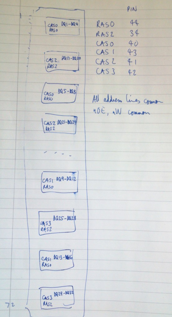
That’s all very useful, but I need to know how the chips are wired up and how the various RAS and CAS lines on the SIMM correspond with the chips themselves. Time for the continuity tester again. A few minutes of beeping reveals the arrangement:

DSC_0276

To summarise:

  • The SIMM is 32 bits wide, and each of the 8 chips handles 4 bits. The 16500A wants 16 bit wide RAM, so half the data pins will have to be commoned together. The layout of the SIMM connector actually makes this quite easy, because the data bits are interleaved in what looks like a handy fashion.
  • the nW line is common to all the chips. The 16500A wants two separate nW lines, so I’ll have to cut the track half way along the SIMM. There seems to be a convenient point under where the parity RAM would be if the SIMM had parity, which it doesn’t.
  • There are two RAS lines used. The 16500A only wants one, so they’ll be commoned together.
  • There are four CAS lines, one for every two chips. The 16500A wants two, so they will be wired as two pairs.

Here’s the plan of action To understand the references to signals in the 16500A, see the previous post.

  • Split nWE half way along the SIMM and connect top half to 16500A W0, bottom half to 16500A W1
  • Connect 16500A CAS0 to SIMM CAS3 and CAS2
  • Connect 16500A CAS1 to SIMM CAS1 and CAS0
  • Connect 16500A D7..D4 to SIMM DQ1..DQ4 and DQ17..DQ20
  • Connect 16500A D3..D0 to SIMM DQ5..DQ8 and DQ21..DQ24
  • Connect 16500A D15..D12 to SIMM DQ9..DQ12 and DQ25..DQ28
  • Connect 16500A D11..D8 to SIMM DQ13..DQ16 and DQ29..DQ32
  • Connect 16500A A9..A0 to SIMM A9..A0
  • Connect 16500A nOE to SIMM nOE
  • Connect 16500A RAS to SIMM RAS0 and RAS2
  • Connect power and ground
  • Cross fingers.

HP 16500A memory upgrade part 1

My HP 16500A has only 1MB of RAM, which isn’t enough to run the system software for the 16550A logic analyzer module I’d like to use in it. Apparently there was a later version of the 16500A which had 2.5MB of RAM, but I haven’t got one of those. Just my luck. Trying to load the 16550A system software results in an error message:

DSC_0273a

This got me thinking. Might I be able to upgrade the memory? The RAM on the 16500A processor board is eight 1Mbit DRAM chips, soldered in:

16500A_RAM

I looked up the data sheet for the chips, TMS44C256. It indicates that pin 5 isn’t used. However, on larger (4Mbit) chips, pin 5 is another address line. Intriguingly, pin 5 is wired up on this processor board, implying that the hardware is ready for larger RAM chips. I have no idea whether the software is ready, but there’s only one way to find out. It’s got to be worth a try, hasn’t it?

Unfortunately I couldn’t find any 4Mbit DRAM chips in the DIL package to fit this board, and making or buying adapters for surface mount chips seems like a pain. However, there is another approach: old PCs are full of SIMM memory modules which have electrically suitable chips on them, and they’re already wired conveniently together. If I removed the 1Mbit DRAM chips from the processor board and string wires from the resulting holes to a SIMM, I might have a 4MB 16500A. Or a doorstop.

To change DRAM chips requires knowing how the address and data buses are wired, and how the RAS and CAS strobe lines are connected to the various chips. RAS and CAS are effectively chip enables, so they can be considered to be part of the address for wiring purposes. A bit of reverse engineering with a continuity tester resulted in this sketch of how the RAM is wired up:

DSC_0253

If I do a similar job on a suitable 72-pin 4MB SIMM, it should be possible to match up the wires and see what happens. There’s a handy vintage SIMM data sheet I found here:

http://www.pjrc.com/mp3/simm/datasheet.html

which should be a good start. What can possibly go wrong?

HP 16500A and 16500B logic analysers

Recently I’ve been putting a couple of HP logic analysis systems into action. Accumulated from various places over the last couple of years I have both a 16500A and a 16500B. They’re remarkable units which take a whole variety of plugins for doing high-speed digital and analogue measurements. They must have been eye-wateringly expensive when new and, as a result, have such high specifications that they’re still useful even though they’re around 20 years old. For example, the 16500B boasts a colour touch-screen, a built-in hard drive and Ethernet. It was launched in 1992 when many desktop PCs didn’t have those features, so it must have seemed awesomely high-tech at the time.

Here’s a picture of the 16500B. The 16500A is similar but looks…older.

DSC_0247s

There are a few quirks to using these machines in 2013, and I’m intending to write about some of my experiences here.

Welcome

Here I’ll be posting technical notes from my workshop from time to time. There will probably be some open source software and hardware for you to help me debug, and almost certainly bits and pieces about old technology which has taught me things I’d like to share.