Author Archives: martinjonestechnology

Henelec PA25 power amplifier and MU442 power supply

Over on the Vintage Radio Forum, someone asked recently about the Henelec PA25 power amplifier module. The PA25 was produced by Henry’s Radio of London in around 1970. Since I have a pair of them, including the associated MU442 power unit, I’ve documented them here.

Here are a couple of general views. The MU442 has sockets for mains in, signal input (3-pin DIN) and speaker outputs (DIN again). There are also a pair of power supply fuses. Connections to the PA25 modules are via wiring harnesses with edge connectors.

Img_3997

IMG_3999


Here’s what one of the modules looks like. It’s a sandwich of a PCB and heatsink.


IMG_4000


This is what’s on the PCB…


IMG_4003

…and on the heatsink…

IMG_4004


…and the back of the PCB.

IMG_4001


The heatsink has a pretty label on it:

Img_4005


This is the MU442.

Img_4006


Inside, there’s a mains transformer with 2x 22VAC secondary windings, four BYZ13N rectifier diodes in stud-mounted packages, and a pair of smoothing capacitors.

Img_4007


I drew out the schematic diagram of the circuit. It’s made with silicon transistors and is pretty conventional, I think,

PA25_Schematic


Here’s a PDF file of it: PA25_Schematic


150W Boost Converter Schematic

In a recent project, I needed a boost converter to step up 5V to about 8V at a few amps. A few different Chinese-made boost converter modules are available from various sources: I’ve seen them on eBay and Amazon. One very common one is known as the ‘150W Boost Converter’. I believe it’s intended for charging laptops from car batteries. It’s specified to take an input of 10-32V and output 12-35V, which isn’t quite what I was looking for, but the price was right so I thought I’d take a chance. This is what I found.

boost

I had a good look at the circuit board. It’s based on the UC3843 chip, which is a pretty old device (I think it dates back to 1984) and is often found in PC power supplies. However, its age and ubiquity means that documentation on it is readily available. I traced out the circuit, so here’s the schematic diagram:

150W_ boost

You can also have it as a PDF file: 150W_ boost.

It’s a pretty straightforward boost converter topology with a MOSFET switching transistor and a variable resistor in the feedback loop to set the output voltage. There is no over-current, over-voltage or reverse polarity protection at all, and the chip isn’t designed for low power consumption so this module wouldn’t be suitable where very low standby power is a requirement. There are a couple of interesting features, though.

The circuit includes an arrangement with an NPN transistor which feeds some bias to the current sense feedback loop. According to the UC3843 datasheet, this improves the stability of the converter at duty cycles higher than 50%.

The control supply for the UC3843 is derived from a 9V regulator, so it’s independent of the input or output voltage. This is convenient.

The UC3843 is designed to operate from fairly high supply voltages, and won’t start up until its supply voltage reaches 8.4V. That was a bit of a problem for my application, where the input voltage was only 5V. However, there’s nothing to say that the chip power supply has to be the same as the power input. In fact, the module already has a handy 9V regulator which feeds the control chip. Looking at the circuit diagram, there are even a pair of resistors (I’ve labelled them R1 and R2) which select whether that regulator is fed from the input or the output. As supplied, R2 was fitted, so the control chip was fed from the output. Here’s a closeup of the relevant part of the board showing R1 and R2.

DSC_0310crop

My application happened to have a low-current 12V supply available, which would be perfect for powering the UC3843. I simply removed R2 and connected my 12V supply to the point where the black arrow is in the photograph. The boost converter now worked perfectly with a 5V input.

I also had to modify it a little to be able to reduce the output voltage below about 11V. R3, labelled in the photo, is part of the feedback network. I simply removed it and replaced it with a piece of wire. Now the output voltage was variable down to 5V, and I was able to set it to the 8V I wanted.

The module seemed very comfortable delivering 3.3A at around 8V, and drew about 5A from the the 5V input. The heatsinks only got slightly warm.

Unfortunately, the power supply I wanted to run the converter and its load from didn’t like starting up with it all connected. This is quite often a problem with boost converters, since the inrush current at startup can be very large as the controller tries to bring the output up to voltage as quickly as possible. I solved this by adding a soft-start circuit to the module. More on that later.

Espial Arcade Game Pinout

espial

Getting through my collection of not-quite-working arcade PCBs, I’ve just sorted out ‘Espial‘ and made a JAMMA adapter for it. In the process, I discovered something missing from the available pinouts of this game online. In the game you have two weapons: you can drop bombs on ground targets, and fire lasers at flying targets. In MAME, the game uses two separate fire buttons, one for each weapon. However, the published PCB pinouts only show one fire button connection for each player. There’s a DIP switch setting which combines both bombs and lasers on to one fire button, which worked for me, but that’s not the same as having separate control of the weapons.

IMG_3734

I set about looking for the second fire button connections. The MAME source code shows that the second fire button for player 1 is in bit 6 of the port at 0x6081, the same port as some of the DIP switches. The inputs all seem to be handled by 74LS368 buffers. Prodding their inputs with a grounded bit of wire during a game revealed that the second fire button for player 1 was on pin 14 of IC2F. Aha! It does exist. Tracing the PCB tracks led me to pin E on the underside of the edge connector via R17. A similar process led me to pin G for the second fire button for player 2.

Here’s my updated version of the pinout diagram:

              COMPONENT  |  SOLDER
    ---------------------+----------------------
               GND   | 1 | A |   GND 
               GND   | 2 | B |   GND
                     | 3 | C |   
               +5V   | 4 | D |   +5V
                     | 5 | E |   1P.Laser
      Coin Counter   | 6 | F |   
           2P.Down   | 7 | G |   2P.Laser
              Coin   | 8 | H |   
           1P.Bomb   | 9 | I |   Service
          1P.Start   |10 | J |   2P.Start
           1P.Left   |11 | K |   1P.Right
             1P.Up   |12 | L |   2P.Up
           2P.Left   |13 | M |   2P.Right
           2P.Bomb   |14 | N |   1P.Down
               GND   |15 | O |   GND
               Red   |16 | P |   Green
              Blue   |17 | Q |   Sync
                     |18 | R |   Speaker
                     |19 | S |   
              +12V   |20 | T |   +12V
               GND   |21 | U |   GND
               GND   |22 | V |   GND

I also found that it was important to connect up all the power and ground connections, even the seemingly duplicated ones, before the game would start up correctly. But start up it does, and it’s fun. I hope this information is useful to someone.

Img_3737

HP 16500A memory upgrade part 7

In part 6, I established that something was stopping the floppy disc drives in my 16500A working when I changed the ROMs to software version 00.02. Thanks to the help of some on the hp-agilent-equipment Yahoo group, especially Glen Slick, I have determined that there’s an important difference between early CPU boards running 00.00 and later ones running 00.02: the floppy disc controller chip has changed!

The old board has an FDC9793 and the new one a uPD765 (or at least its Zilog equivalent). There are pictures of all the boards here. Now, I started to wonder, could I somehow fit the uPD765 to my board? It seems crazy and would only make sense if it wasn’t possible to exchange the whole board. So I started investigate. As luck would have it I have a functional 16500B with a logic analyzer plugin, so I could have a look and see what was going on around the disc controller on my CPU board. I wired up the relevant pins of the FDC9793.

DSC_0305

Examining the logic analyzer trace, it seems that the CPU is trying to read something from the disc controller, which is at least a start.

DSC_0304

It’s reading from what would be the status register repeatedly, as if waiting for some condition to be true. It gets a value of 0x04 every time, which is presumably not what it wants. It does this at the right stage of the self-test. I thought this was promising, since it is at least addressing the chip. Might it be possible to wire one in place of the other? Their pinouts are different. Comparing them, using their datasheets:

FDC9793 uPD765
1 RESET I active high
2 nWE I nRD I
3 nCS I nWR I
4 nRE I nCS I
5 A0 I D/nS I data/nStatus register select
6 A1 I D0 I/O
7 D0 I/O D1 I/O
8 D1 I/O D2 I/O
9 D2 I/O D3 I/O
10 D3 I/O D4 I/O
11 D4 I/O D5 I/O
12 D5 I/O D6 I/O
13 D6 I/O D7 I/O
14 D7 I/O DRQ O DMA request
15 STEP O Step output nDACK I DMA ack
16 DIRC O Direction (high=in, low=out) TC I end of DMA transfer
17 EARLY O write precompensation IDX I index pulse
18 LATE O write precompensation INT O interrupt output
19 nMR I master reset CLK I 8MHz
20 GND GND
21 +5V WCK I write clock
22 nTEST I tie to +5V RDW I read data window
23 HLT I input, head engaged RDD I read data from data sep
24 CLK I 1MHz in VCO/SYNC O enable VCO
25 RG O read gate to data sep WE O write enable
26 RCLK I read clock from data sep MFM O MFM/FM
27 nRAW READ I raw data from drive HD O head select
28 HLD O head load US1 O unit select
29 TG43 O track greater than 43 US0 O unit select
30 WG O write gate WDA O write data
31 WD O write data PS1 O precompensation shift (early/late/normal)
32 READY I ready PS0 O precompensation shift (early/late/normal)
33 nWF I/O write fault/vfo en to data sep FLT/TR0 I track 0/fault
34 nTR00 I track 0 WP/TS I write protect/two side
35 nIP I index pulse RDY I drive ready
36 nWPRT I write protect HDL O head load
37 nDDEN I double density FR/STP O fault reset/step
38 DRQ data req, open-collector LCT/DIR O low current/direction
39 INTRQ interrupt req, open-collector nRW/SEEK O indicates seek/read/write mode
40 +5V

There are some important differences here. Firstly, the uPD765 expects an 8MHz clock where the FDC9793 used a 1MHz clock. That’s not a good start. The uPD765 includes drive and side select logic, but the FDC9793 doesn’t. The two also differ a lot in how they handle things like write precompensation signals, and the uPD765 effectively multiplexes various signals too.

At this point I think the swap is just too difficult. It becomes cheaper and easier to swap the whole CPU board, if I can find one, or simply upgrade the whole machine to be a 16500B.

HP 16500A CPU board versions

As part of my quest to upgrade my HP 16500A logic analyser’s memory, I’ve found out more than I ever expected about the various versions of the 16500A CPU board. I’ve been fortunate to have the help of the good people of the [hp_agilent_equipment] Yahoo! group. My most recent stumbling block has been that installing ROM version 00.02 in my (early) 16500A stops the floppy disc drives working.

Glen Slick, from the above group, was kind enough to send me high-resolution scans of the two 16500A CPU boards he has. That makes three known versions, and here I’ll post pictures of them and attempt a description of the differences.

16500-66503 with 1MB RAM

DSC_0262

This is the board from my machine. It has 1MB RAM in 8 TMS44C256-12N DIL chips, and the floppy disc controller is a Standard Microsystems FDC9793. The ROMs contain software version 00.00. For completists, I have put images of the V00.00 16500A ROMs here.

16500-66507 with 2.5MB RAM

16500-66507-FRONT

This is one of Glen’s boards. It has 2.5MB RAM fitted as 20 off TC514256AZ-10 1Mbit ZIP chips, and the floppy disc controller is a Zilog Z0765A (which seems to be compatible with the very common uPD765 as found in the original IBM PC). The ROMs contain software version 00.02. It also has three extra programmable devices with labels on them. The details of their encapsulation mouldings look very similar to PALs elsewhere on the board, but why don’t all the PALs have labels on them? The labelled ones are:

  • 16500-80006, U86, by the floppy drive connector at the bottom
  • 16500-80007, U104, top right
  • 16500-80008, no designator visible, next to the floppy controller IC

16500-66510 with 4MB RAM

16500-66510-FRONT

This is another of Glen’s boards. The part number (66510) seems to be on a sticker. The only noticeable difference, other than the RAM chip complement, from the 66507 board is that the chip top right is labelled 16500-80013. It has 4MB of RAM as 8 off TC514400AZ-80 4Mbit ZIP chips. The ROMs contain software version 00.02.

Using a 32.768kHz external crystal with Atmel XMEGA microcontroller RTC

I’ve just brought up a project using an Atmel XMEGA series microcontroller which uses an external 32.768kHz crystal to run its real time clock (RTC). I had some trouble getting it to work, but now I’ve found the recipe, thought I’d share it in case it’s useful to anyone.

DSC_0308

In principle, you’re supposed to enable the crystal oscillator and then wait until the XOSCRDY bit is set in the OSC.STATUS register, indicating that the oscillator has started up. My problem was that the oscillator seemed to be running, with a healthy-looking waveform at the XTAL1/TOSC1 pin, but the ready bit never got set.

DSC_0309

It turns out that the order of initialising the registers is important. You have to set XOSCCTRL first, to configure the oscillator, then enable it in CTRL, then wait for it to be ready. The code looks like this

OSC.XOSCCTRL= OSC_XOSCSEL_32KHz_gc;
OSC.CTRL|=OSC_XOSCEN_bm;
while(!(OSC.STATUS&OSC_XOSCRDY_bm));

That’s what worked for me. I’m using AVR Studio 6 and AVRGCC version 3.4.1.95.

Bubble Development Board V1.0

I’ve just got V1.0 of a development board for the ‘Bubble’ embedded ARM module ready for manufacture, and will hopefully have prototypes soon.

BubbleDevBoard1.0

It’s designed to make the Bubble board easy to work with, and brings out various useful connectors:

  • JTAG ports compatible with Xilinx (14-pin) and ARM (20-pin) dongle pinouts
  • Serial port for the console
  • USB host, for memory sticks, keyboards and whatever else
  • USB slave, for mass storage or USB networking
  • Micro SD card
  • HDMI for monitor connection
  • Ethernet
  • Stereo analogue audio in/out
  • Raspberry-Pi compatible expansion connector with I2C, SPI and GPIO

It’s all powered from a Micro USB connector which should take a standard mobile phone charger, and is designed to sit neatly in a low-cost plastic box for protection.

Everything except the Ethernet port is already supported by Linux on the Bubble board, though making the HDMI port work will involve some fiddling with the LCD output timings. The Ethernet port is based on the Wiznet W5100 chip, which is popular in the embedded community and is supported by recent Linux kernels.

Super Pacman repair log

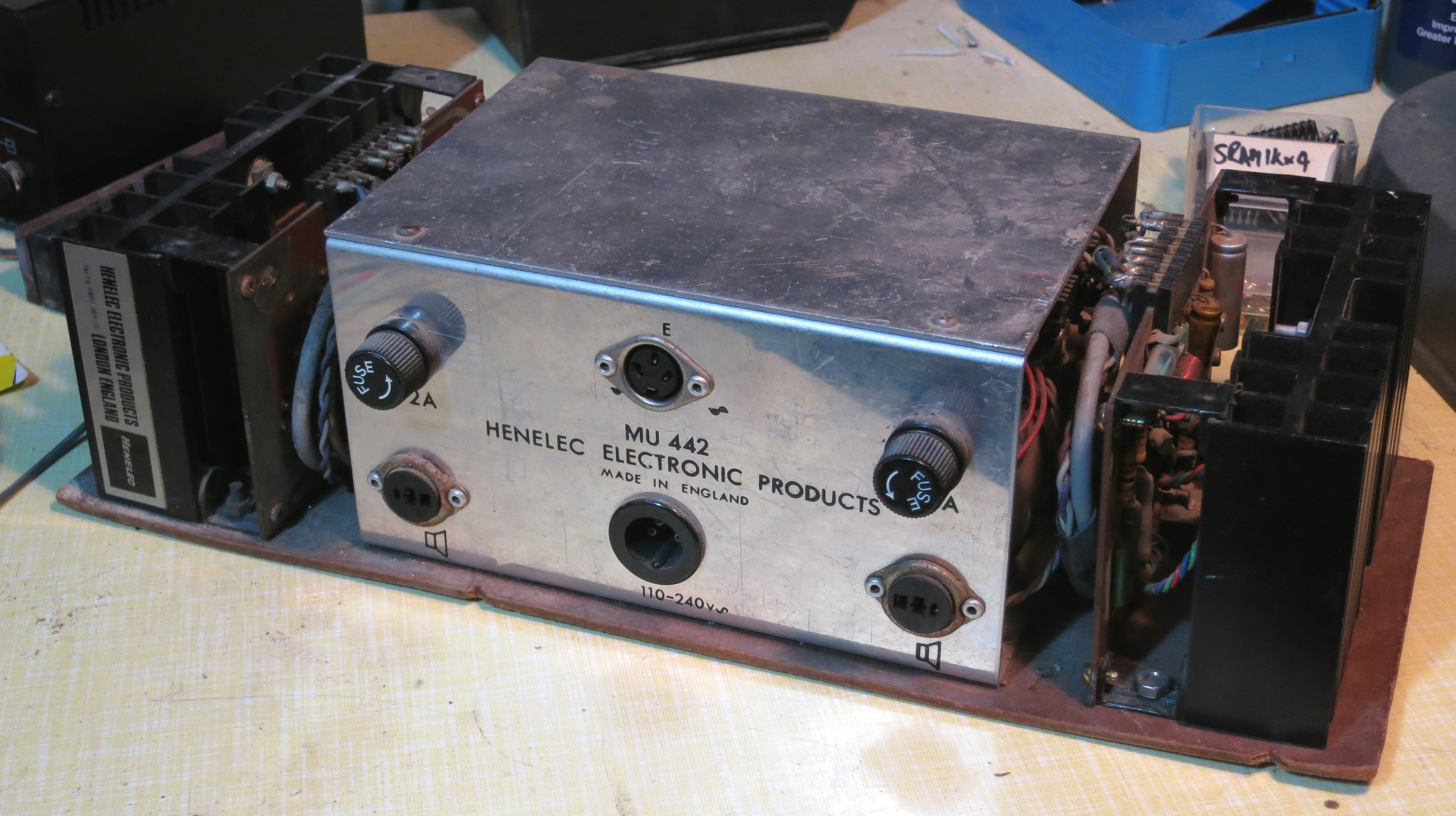
I’ve just got an old Super Pacman arcade game running. Not the whole cabinet, you understand, which would be inconveniently large, but the circuit board from inside one, connected up to a monitor and joystick.It’s the lesser-known 1982 sequel to Pacman and Ms Pacman. It’s a fun game, with more complicated gameplay than the original: gates, keys, a speed-up button and a special powerup which makes you really big and able to go charging through everything. I could find hardly any repair information about Super Pacman on the internet, so I thought I’d paste my repair log here so people can see it.

Firstly, as part of the process, I pasted together large high-resolution circuit diagrams by cutting and pasting from the available PDFs of the manual in which they’re sliced up into pages. The ones I’ve stuck together are more convenient to use when printed out on large sheets of paper or viewed on a big screen. I hope they’re useful.

super-pacman-cpu-hires

super-pacman-graphics-hires

Super Pacman repair log

1/1/2013

Connect up power and video. Occasional flashes of something on the screen but no sync. Main clock oscillator is running.

Lack of sync output seems to be due to unenthusiastic 74LS10 at 3A. Output at pin 12 is weak. Vertical sync input at pin 13 is OK but H sync input at pins 1 and 2 is very poor – barely leaving +5V but pulses are visible. Comes from a custom chip 2C. Hope it’s not knackered. Cut pins of LS10.
Output of custom recovers.

Replace 3A. Now we have a picture of random junk in blue and green which wriggles a bit when reset button is pressed.

Why does there appear to be no red in the picture? There’s activity on R video pin even though pin 1 of colour PROM 4C has snapped off. Maybe a blanking problem.

2/1/2013
RGB outputs are high during what should be blanking interval. Investigate inputs to PAL 4D. 6/7/8/9 are all stuck high. They come from 74LS298 4L, whose inputs looks pretty sensible but outputs are all stuck high. Remove it ready for replacement.

Blanking signal from 3A pin 6 ends up at PAL 4D pin 19 and seems to force its outputs to 01111. In this state, output of colour PROM 4C is 10101111. That’s definitely wrong according to the MAME ROM image. Should be 00000000.

Can’t buy or program PROMs easily so try substituting with a high-speed OTP PROM: Atmel 27C512. Physically large but cheap and easy to program, 45ns access time is OK. Wiring:

82S123 27C512
O1   1  O0  11
O2   2  O1  12
O3   3  O2  13
O4   4  O3  15
O5   5  O4  16
O6   6  O5  17
O7   7  O6  18
GND  8  GND 14, 1,2,3,4,5,21,22,23,24,25,26,27
O8   9  O7  19
A0  10  A0  10
A1  11  A1   9
A2  12  A2   8
A3  13  A3   7
A4  14  A4   6
nCE 15  nCE 20
VCC 16  VCC 28

Now colours are sensible. Maybe 4L (74LS298) isn’t faulty after all – It might just be that no sprites are displayed so there’s no activity.

IMG_3556

PROM at 4E is losing pin 1. Need to sort it out.

10/1/2013
Try and work out why game doesn’t run. Activity on data and address buses. EPROMs 1 and 2 (1B and 1C on CPU board) verify OK. When it stops, it’s resetting the watchdog continuously!

Sound CPU isn’t running cos its reset input (37) is low. Comes from latch 2M (74SL259). Pulling it high for a moment makes it stay high, oddly.

15/1/2013
Repair pin 1 of PROM 4E with Dremel and bit of wire. Screen of random characters looks more and more sensible: the word ‘CREDIT’, or bits of it, seem to be appearing in places.

Replace suspect 74LS298 at 4L now replacements have arrived. Makes no difference at all.

18/1/2013
Start examining buses and their buffers. Buffered address bus (from CPU board 2H, 1H, 1E) looks OK but buffered data bus has some bits hanging around near 0 where they should be pulled high. Disconnect the two boards and the fault is definitely on the video board. Could be any of 74LS245 1E, 1K, 1J, 1H. Remove them all. Replace them with secondhand chips. Board still doesn’t run but pattern on screen is somehow a bit different. RAM fault? Piggybacking RAMs doesn’t have any
effect.

19/1/2013
Chip at 2E (Namco 04xx) seems to be associated with addressing the RAMs. We have replacements on some Pole Position boards. Try swapping it and results are definitely different: instead of just random characters, there are now random sprites as well. Try two different 04xxs (0429 and 0436) from Pole Position and they both behave the same. Assume they’re OK then
and the original is faulty. Game still doesn’t run. Can’t see any dodgy logic levels on video board and piggybacking RAMs doesn’t help.

Still no interrupts happening. 74LS259 at 2M on CPU board is behaving oddly. It is being addressed but none of its outputs are changing, but if I pull any of them high for a moment they stay high.

When CPU crashes, it sits in an 8-cycle loop. Record what’s going on.

A EEEEEEE8
  11F111F0
  77F777F0
  BCF89AF0
D 2F0B8003
  0B070001

A15 11111111
A14 11111110
A13 11111110
A12 00100010
A11 00100010
A10 00100010
A9 00100010
A8 11111110
A7 00100010
A6 11111110
A5 11111110
A4 11111110
A3 11111110
A2 01100010
A1 10100110
A0 10101010
D7 01011000
D6 01000000
D5 11010001
D4 01010001
D3 01000000
D2 00010000
D1 01010000
D0 01010001
RnW 11111110

It’s in a tight loop at E178-E17F, which finishes by writing the value 0x31 to 0x8000. That’s the address which resets the watchdog.

Analysing the code in MAME, it seems that the first part is a RAM test which copies the ROM (from E000 onwards) into the RAM and reads it back, comparing it with the ROM. If it fails, it will try to put up the self-test screen indicating which RAM has failed, then go into the loop at E178. A value of 0x31 in A I think indicates that the tilemap RAM has failed, at 2E on the video board. So it seems that the first RAM test is failing and it’s trying to tell us about it, but access to the video RAM is so broken that we can’t see it. The CPU is actually running correctly.

Replace RAM 2E. Doesn’t make any difference, but if I remove buffer 1E the screen should clear with after the RAM test. It doesn’t, and behaves a bit randomly. Remove custom 00xx at 2D, which is the video address generator and thus has the ability to mess up video RAM addressing, and game appears to run! But tilemap is all the same character, not surprisingly because nothing’s generating video addresses. Pin 1 has dropped off 00xx. Temporarily connect it with scalpel and we have action. Repair pin 1 properly and game runs.

Try inserting coins by tickling edge connector with grounded wire. We can start a game and control Pacman. Pinout seems to be the same as Grobda but with player 1 and player 2 swapped over.

Wire up single player JAMMA adapter. Sound works! Pleasant surprise. Some sprites sometimes become white squares, but reseating customs on video board solves the problem.
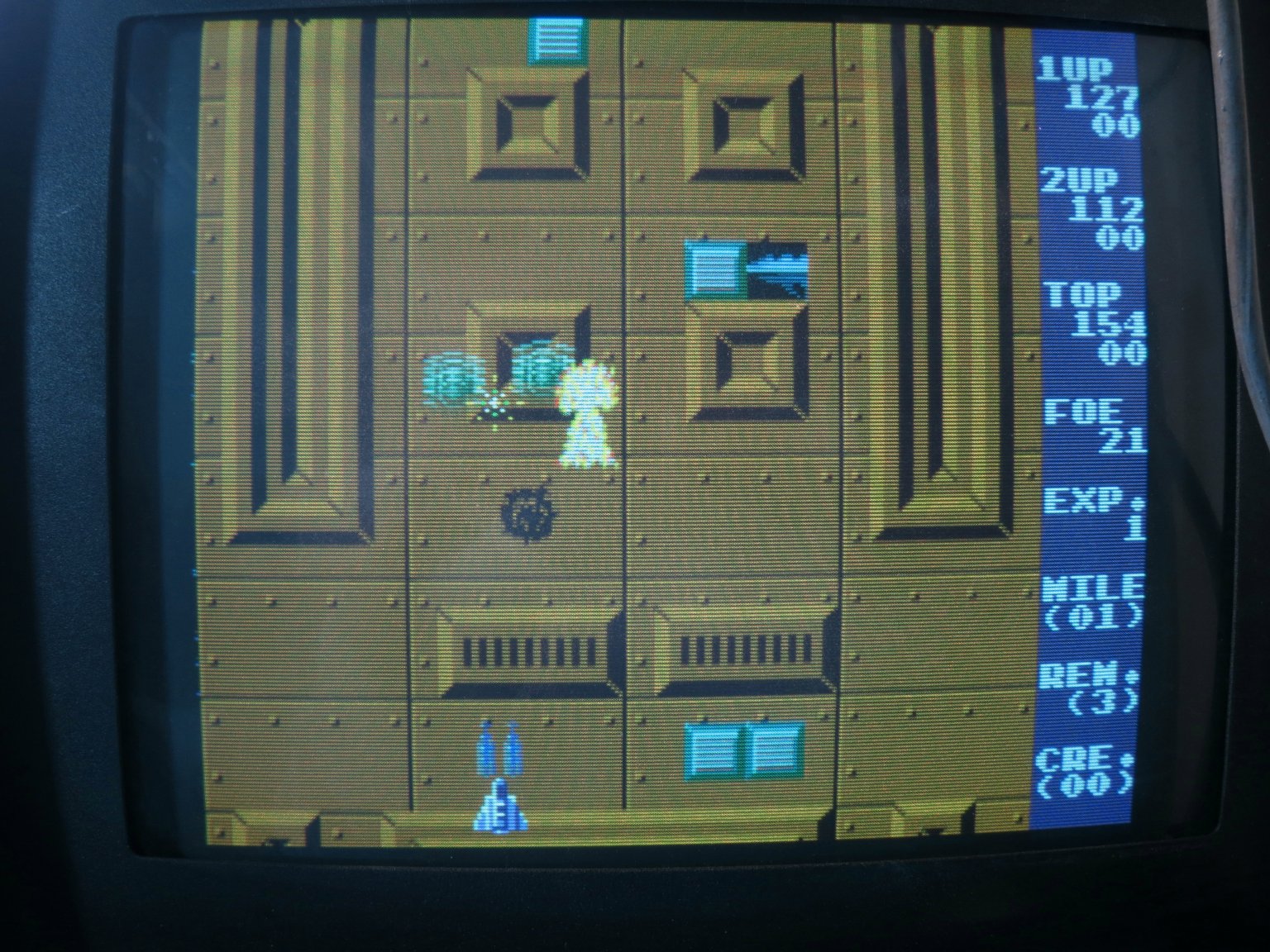
Game fixed.

Img_3558

HP 16500A memory upgrade part 6

In part 5, upgrading the software on my 16500A’s CPU board to version 00.02 resulted in a self-test failure, which wasn’t fixed by downgrading back to 00.00. I’ve just had a look to see why that was happening.

The front panel is connected to the backplane by a 10-way connector. I traced out the pinout of the connector:

  1. +5V power
  2. +12V power
  3. +5V power
  4. +12V power
  5. Ground
  6. Data
  7. Ground
  8. Data
  9. Ground
  10. On/off switch, ground to switch system off

There was no activity at all on pins 6 and 8, the data pins, even during self-test. I traced them through to the CPU board via pins 59 and 60 of the CPU board’s backplane connector, and thence to U90 pins 18 and 19. This is an HP custom chip. There seemed to be activity on many of its pins, but nothing on those two. Poking around, I found that two of its pins are connected to a nearby ceramic resonator which clearly wasn’t resonating. Aha! Got it. One of the pins of the resonator had broken. I soldered it back together and now the self-tests pass!

But there’s a fly in the ointment. V00.02 software doesn’t seem to be able to access the floppy disc drives, simply reporting ‘No Disc’ for both of them even when they’ve got discs in.

Looking at the floppy disc connector with a scope, the ‘drive select’ pins are definitely active. It seems that the pinout of Sony 3.5″ floppy disc drives changed at some point. The details are here:

http://www.retrotechnology.com/herbs_stuff/drive.html#35new

Pin#  Signal (Old Sony)  Signal (New Sony)  Pin#  Signal (Old Sony)        Signal (New Sony)
1     Disc Change Reset   NC                2     Disc Change Indicator    NC
3     +5V                 Key               4     Density Bit              NC
5     +5V                 Ground            6     Drive Select             NC
7     +5V                 Ground            8     Index Pulse              Index
9     +5V                 Ground            10    Drive Select 0           NC
11    +5V                 Ground            12    Drive Select 1           Drive Select 1
13    Ground              Ground            14    Drive Select 2           NC
15    Ground              Ground            16    Motor On                 Motor On
17    Ground              Ground            18    Direction Select         Direction
19    Ground              Ground            20    Step                     Step
21    Ground              Ground            22    Write Data               Write Data
23    Ground              Ground            24    Write Gate               Write Gate
25    Ground              Ground            26    Track 0 Indicator        Track 00
27    Ground              Ground            28    Write Protect Indicator  Write Protect
29    +12V                Ground            30    Read Data                Read Data
31    +12V                Ground            32    Head Select              Head 1 Select
33    +12V                Ground            34    Ready                    Disc Change

It seems that the ‘disc change indicator’ has moved at some point in the history of Sony disc drives. Maybe the new software is expecting to see the ‘disc change’ indicator before it tries to switch the drive motors on? Grounding pin 34 doesn’t seem to make any difference. The disc controller is an FDC9793. Looking up the data sheet on it, it doesn’t have any means of indicating whether a disc is in or not. Without a schematic, it’s going to be very hard to figure out how the software determines it.

HP 16500A memory upgrade part 5


Following on from part 4, I’ve now tried a newer software version in the 16500A’s EPROMs. Finding a couple of good 27C256s with 200ns access time took a few minutes, but there were no problems with the programming. So, I put them in the CPU board, reinstalled it in the mainframe, and switched on:imageOh dear. That’s not good. Without HIL (which is the socket for mouse and keyboard on the front), front panel (which I assume is the spinner knob) or touchscreen, the machine isn’t a lot of use. Must be a compatibility problem with the new software version, I think to myself. Swap in the old ROMs – and the problem is still there. Check the wiring to the front panel, all looks good.

This is annoying. I wasn’t expecting new faults with the hardware. When I next get time to spend on it, I’ll do the obvious checks for bent pins and so on.