This little thing is really annoying. It’s the remote control for our electric garage door, and I use it several times a day to get my bike in and out. Luxury, pure luxury. Or it would be, if it worked properly. The trouble is that about half the time after pressing the button, it locks up, stuck either on, with its little red LED lit, or off, so it won’t open or close the door, and drains the battery. The only way to fix it is to pull it apart, take out the battery, and put it back in without losing any of the bits of plastic. You can imagine how much fun that is with gloves on, in the rain, when you’re in a hurry. Yeah, yeah, first world problems, I know. But there doesn’t seem to be any way of opening our garage door manually, which is a nuisance.
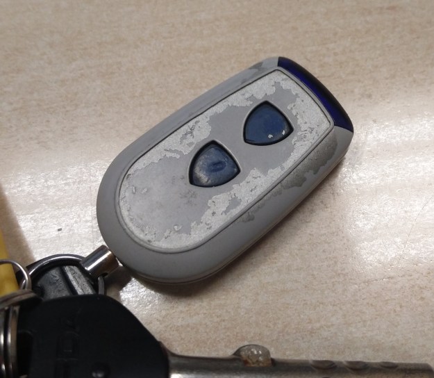
Inside is a little PCB containing a PIC12F635 microcontroller and a simple 433MHz transmitter circuit using a couple of transistors and a resonator. I did all the obvious things: replace the battery, clean the board with solvent, all of that. Nothing helped. It seems there’s a bug in the PIC’s software which makes it prone to locking up. The switch under the button is rather worn and thus suffers from contact bounce, and I think that’s what’s upsetting it.
I tried filtering the signal from the button to the PIC with an RC network. That didn’t help: the PIC didn’t even respond to the button any more. Presumably it needs a fairly quick risetime to trigger an interrupt, or something similar.
There is a second button which is less worn. It transmits a different code which doesn’t seem to do anything on our garage door, but it never crashes the PIC. I considered swapping the switches over, but they’re surface-mount and glued down, and the chances of removing both of them and successfully soldering them down again undamaged were slim.
I wondered about rewiring the PCB so that the input to the PIC is always active, and the button just switches the power to the PIC. A quick test by adding a blob of solder and removing and reconnecting the battery showed that wasn’t going to work: the PIC just didn’t transmit. It needed to have the power applied and then have the button activated.
There was another issue to address. The button, when it worked, was prone to getting pressed by accident as the bunch of keys rattled around in my pocket. That led to the garage door opening itself at odd times, which wasn’t great for the security of our bikes. Somehow modifying it to be less prone to accidental operation would be nice.
Design changes were called for. Since the second button is redundant, I decided to convert it in to a power switch, so it has to be held down while the real button is pressed, and releasing it will guarantee that the power is cut from the PIC so it can’t remain locked up. I cut the power track to the PIC and took advantage of the PCB layout to add a P-channel MOSFET in series with it, then cut the track from the second button to the PIC’s input and wired it to the MOSFET’s gate. The buttons both have one terminal to battery negative. A pullup resistor between gate and source completes the circuit.

Here’s the modified board. You can see the remnants of some of my previous repair attempts, and the extra MOSFET and pullup resistor at top right. Now, to open or shut the door, I have to hold down the button on the right and press the left button, rather like using a shift key on a keyboard.
It seems to work reliably now, so leaving the house and returning are considerably quicker and less stressful.
Incidentally, I did the repairs and modifications in the office, which is several miles away from the offending garage door. To check that the remote was actually transmitting properly, I used my Tektronix 7912AD programmable digitizer with 7A29 vertical plugin. Originally intended for high-speed laser and nuclear physics research, it’s kind of overkill for testing a garage door opener, but its 700MHz bandwidth is plenty fast enough to get a clear picture of the transmission using just a loop of wire connected to the input. Analogue technology at its very finest. Here’s its TV output connected to a little LCD monitor showing the 433MHz signal from the remote.